Keywords
|
| Static CMOS Logic, Domino Logic, Feedthrough Logic (FTL), Low Power. |
INTRODUCTION
|
| In the fast growing VLSI industry transistor density per chip is increasing day by day following the Moore’s law. With increase in transistor density, area and power consumption also increases. The design engineers are striving to achieve more and more functionality at higher speed and low power, keeping area and cost low. Circuit design techniques also plays an important role in achieving high performance, low power or low area. Design engineers can consider different logic design techniques according to the need of their design. Some designs need to be very fast despite of area and power dissipation, example in some real time systems, while some requires very low power and small area, as in like portable devices. In this paper different logic design techniques are discussed and a comparative analysis has been done between them for power and speed. All the design techniques have their own characteristics, advantages and drawbacks. For example in static CMOS circuits power dissipation is low but are very slow and implementation area is large as compared to domino. On the other hand dynamic logic circuits are very fast and have low area but dissipate more dynamic power as compared to static CMOS logic. There are some other proposed techniques such as feedthrough logic (FTL) and low power FTL which further improves the characteristics of domino logic and also solves many problems of domino logic such as non inverting logic, use of inverter at the output and charge sharing etc. One another proposed technique called zigzag keeper is also discussed here which reduces the power dissipation largely but at the cost of area overhead. At last, between these techniques a comparative analysis has been done based on literature survey and previous papers, so that to make it easy to select from these different techniques according to the need. |
STATIC CMOS LOGIC
|
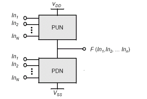
| Static CMOS logic is the most commonly used logic design technique. In this circuit are made up of two networks namely pull up network (PUN) and pull down network (PDN) (Fig. 1). PUN consists of PMOS transistors and PDN consists of NMOS transistors. Input to these networks is dual of each other. Output is connected to power supply or ground based on the inputs applied to PUN and PDN making the output 1 or 0 respectively [1][2]. |
| One of the advantages of Static CMOS circuits is that they have high noise margin so they are more scalable than dynamic logic. Therefore threshold voltage of transistors can be lower than dynamic logic circuits. So performance of circuits can be improved which are designed for ultra low voltage [6]. In steady state mode there is no direct path between VDD and ground so power dissipation is only due to leakage current in transistors. |
| The main drawback of static CMOS logic is that it uses more number of PMOS transistors which increases the delay and area of the circuit. To design a logic gate with n inputs, 2n transistors are required which results in large area of the circuit. And in some logic implementations PMOS transistors occurs in series due to which input capacitances increases and the output driving capability of the circuit reduces . Also in these circuits in some logic implementations, different paths have different delays, so glitches or spurious transitions can occur . For large fan-in gates performance of this logic family is not very good [2][3][4]. |
DOMINO LOGIC
|
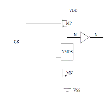
| Domino logic design technique is the improved version of dynamic logic family. Fig. 2 shows domino logic which consists of a dynamic logic circuit followed by a static CMOS inverter. This circuit consists of a PMOS pre-charge transistor MP and an NMOS evaluation transistor MN with their gates connected to clock, and there is an NMOS logic network which implements the required logic function. During the pre-charge phase (Clock = 0) the output of the circuit get charged through the pre-charge transistor MP to the level of VDD and the output of inverter is low. Now during the evaluation phase (Clock = 1) the evaluation transistor MN is ON, and the output of the dynamic circuit either discharges to ground or remains at high level depending on the inputs applied to the NMOS network. |
| In circuits of domino logic there can be other capacitive nodes in NMOS block which shares the charge of the output node capacitance, which decreases the output voltage level, this problem is called charge sharing[1][3]. |
| One of the major advantages of the domino logic over the static CMOS is that this works on high frequency clock and there is no PUN so this eliminates the spurious transitions and corresponding power dissipation. But in some logical conditions output is pre-charged only to discharge in the evaluation phase, for example, if output is low and we apply inputs which gives low output then in pre-charge phase the output will charge to high voltage and during evaluation phase it will discharge to low, increasing the power dissipation. Therefore, the signal activity increases for this circuit design technique and this increased signal activity along with the extra load that the clock line has to derive are the main reasons for high power dissipation in domino logic as compared to static CMOS circuits. Noise margin of Domino logic circuits is low as compared to static CMOS circuits so they are not as scalable as static CMOS. So transistor threshold voltage is kept high to reduce leakage in domino logic circuits. As compared to static CMOS area is reduced in domino logic circuits because of the reduced number of PMOS transistors. Also there is no short circuit power dissipation in domino and they have strong output driving capability [2][5][6]. |
FEEDTHROUGH LOGIC (FTL)
|
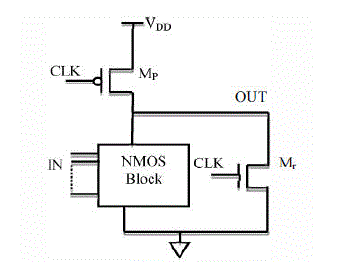
| Feedthrough logic is shown in fig. 3. This logic circuit consists of a PMOS load transistor Mp and an NMOS reset transistor Mr and an NMOS block in which inputs are applied. The gates of the load transistor and the reset transistor are connected to clock. When clock =1(reset phase) load transistor Mp is OFF and reset transistor Mr is ON and the output is reset to logic low. Now when clock =0(evaluation phase) load transistor Mp is ON and reset transistor Mr is OFF and the output either goes to logic level high or remains at low logic according to the inputs applied to the NMOS block. So in this output can either go from 0 to 1 or remain at 0 level according to the applied inputs. |
| In FTL the output logic level is evaluated before all the inputs are valid, so its speed is very high. The problems in domino logic circuits like charge sharing and use of inverter at the output are also solved. |
| In domino logic an inverter is needed at the output during cascading and the output is charged to VDD so there is high dynamic power dissipation but in FTL output is reset to low before evaluation during reset phase eliminating the requirement of inverter for cascading. The performance analysis of a chain of 10 inverters using FTL in [10] shows that when clock =1 the output of each stage goes to logic 0 and when clock =0, voltage at the output node of the cascaded gate rises to threshold voltage of the gate and then if input changes, the output makes transition from threshold voltage to high level or low level. So in this as transition is from threshold voltage to high or low level, the speed is increased to a greater extent. But in this logic there is more power dissipation because minimum output low voltage is not 0V. Noise margin is reduced in FTL [7][8]. |
LOW POWER FEEDTHROUGH LOGIC (LP-FTL)
|
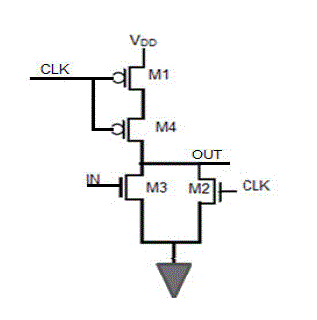
| The LP-FTL circuit is shown in Fig. 4. In this circuit an additional PMOS transistor M4 is introduced in series with M1. When clock =1 (reset phase) M2 is ON and M1 and M4 are OFF so the output is discharged to logic low. When clock =0 (evaluation phase) M1 and M4 are ON and M2 is OFF so the output is evaluated according to the applied input. In this circuit as M1 and M4 are in series so the voltage at the drain of M1 is less than VDD and due to this the minimum output low voltage VOL is less than the VOL of FTL. Due to this reduction in VOL dynamic power dissipation of the circuit is reduced but use of M4 increases delay. |
| In this logic design technique the output can makes transition from 0 to 1 or remains at 0 but in domino it is reverse so an inverter is used at the output in domino (to make initial inputs 0 for next stage to make proper functioning of stages in cascading ). So this technique also solves the problem of using inverter at the output of domino logic. Power consumption of this circuit is improved to a good extent as compared to FTL but in this circuit some delay is increased [7][8][9]. |
ZIGZAG KEEPER
|
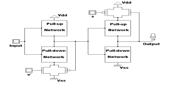
| Zigzag keeper uses techniques of both sleep transistor and keeper transistor with zigzag approach (fig. 5). Sleep transistors are connected to sleep signal through gate and the gate of keeper transistor are connected to the output of the circuit. During sleep mode, the sleep transistors are turned OFF so preserves the state and prevent any leakage. The keeper transistors are connected to the output of the circuit so during sleep mode they are ON or OFF according to the output to preserve the state. For example if there is high output in second stage then the keeper NMOS transistor will turn ON saving the state of the circuit. In sleep transistor technique the pull-up network and pull-down network are taken of low threshold voltage and sleep transistor is taken of high threshold voltage so in sleep mode sleep transistors will be OFF and as they are of high threshold voltage, they prevent leakage and saves the power[2][10]. |
| Power dissipation in zigzag keeper technique is very low as compared to other logic design techniques such as static CMOS and it reduces as process technology is scaled down [10]. The disadvantage of this logic design technique is that the area is increased largely. |
COMPARISON
|
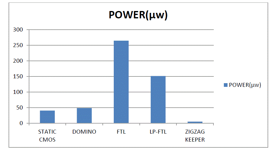
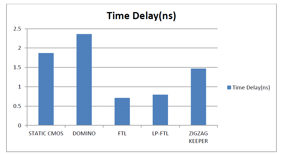
| In this section different design techniques are compared as illustrated in table 1 and fig. 6,7. As static CMOS technique has low power dissipation but its time delay is very large and area of implementation is also large. This problem of low speed of static CMOS circuits is solved by domino logic. Another advantage of domino logic is that its area is reduced as PUN network is replaced by only one PMOS transistor with clock at its gate but its dynamic power dissipation is high. |
| We can see from fig. 6 and 7 that Feedthrough logic improves the speed of the domino logic but it dissipates more power. Then LP-FTL was introduced to improves the power consumption of FTL logic and from fig. 6 we can observe that it dissipates much less power than FTL but fig. 7 shows that its delay increases. We also observed that zigzag keeper dissipates less power than other techniques. But its area is very high. |
| This comparison for power and delay of different techniques is done for a chain of 10 inverters. The results can vary for any other circuit design. |
CONCLUSION
|
| In this paper different logic design techniques were discussed and compared for power, delay and area. Static CMOS and zigzag keeper are good where low power is required and speed and area are not considered. Zigzag keeper has very low power dissipation than Static CMOS but Static CMOS has low area than zigzag keeper. Whereas domino logic and LP-FTL are good where speed is the primary concern. LP-FTL has good speed than domino and also solves the problems of domino logic such as non-inverting logic, charge sharing, need of inverter at output etc. but its area is greater than domino. So this comparison of these different logic design techniques can make it easy for someone to choose logic design technique according to the need of design. |
| |
Tables at a glance
|
 |
| Table 1 |
|
| |
Figures at a glance
|
 |
 |
 |
 |
| Figure 1 |
Figure 2 |
Figure 3 |
Figure 4 |
| |
 |
 |
 |
| Figure 5 |
Figure 6 |
Figure 7 |
|
| |
References
|
- J.M. Rabaey, A. Chandrakasan, B. Nikolic, 'Digital Integrated Circuits: A Design perspective' 2e Prentice-Hall, Upper saddle River, NJ, 2002.
- Kaushik Roy, Sharat C. Prasad , " Low-Power CMOS VLSI Circuit Design", John Wiley & Sons, 2009.
- Neil H.E. Weste, David Harris and Ayan Banerjee, "CMOS VLSI Design, A circuits and system perspective", (3rd Edition, Pearson Education,2005).
- John P. Uyemura, "CMOS Logic Circuit Design", Springer, 1999.
- N. Srinivasa Gupta, M. Satyanarayana, " A Novel Domino Logic for Arithmetic Circuits ", International Journal of Innovative Technology andExploring Engineering (IJITEE) ISSN: 2278-3075, Volume-3, Issue-3, August 2013.
- S. M. Kang, Y. Leblebici, 'CMOS Digital Integrated Circuits: Analysis & Design', TATA McGraw- Hill Publication, 3e, 2003.
- V. Navarro-Botello, J. A. Montiel-Nelson, and S. Nooshabadi, “Analysis of high performance fast feedthrough logic families in CMOS,”IEEETrans. Cir. & syst. II, vol. 54, no. 6, Jun. 2007, pp. 489-493.
- Sauvagya Ranjan Sahoo, Kamala Kanta Mahapatra," Performance Analysis of Modified Feedthrough Logic for Low Power and High Speed",IEEE-International Conference On Advances In Engineering, Science And Management (ICAESM -2012) March 30, 31, 2012.
- Sauvagya Ranjan Sahoo , Kamala Kanta Mahapatra," An Improved Feedthrough Logic for Low Power Circuit Design", 1st Int’l Conf. on RecentAdvances in Information Technology | RAIT-2012 |
- Kaushal Kumar Nigam, Ashok Tiwari, ?Zigzag Keeper: A new approach for low power CMOS circuits", International Journal of AdvancedResearch in Computer and Communication Engineering Vol. 1, Issue 9, November 2012.
|