Keywords
|
| Boost converter, MOSFET, coupled inductor, Photovoltaic system. |
INTRODUCTION
|
| Renewable energy attracts interest for power generation because the non renewable energy like petrol, diesels etc are diminishing and energy crisis is an important concern in most of the nations.In renewable energy, solar energy attracts more because it has more advantage compare to other renewable energy s like the selection of area is not complicated, the systems can either be operated as isolated systems or connected to the grid as a part of an integrated system, it has no moving parts; it has a long lifetime and low maintenance requirements and most importantly it is one solution that offers eco friendly power [11]. Photovoltaic system requires a power electronics interface to be connected to the grid. The most commonly used dc/dc converter is a boost converter which provides an acceptable voltage conversion ratio and also requests a continuous current from the power source [1]. The characteristics required in photovoltaic applications are low current ripple injected to the power source and high conversion efficiency. In the photovoltaic case, the current ripple impacts the power generation since it produces an oscillation around the Maximum Power Point (MPP) reducing the energy extracted from the photovoltaic generator [9]. Those characteristics make the boost converter a good candidate to interface the photovoltaic systems. Additionally it requires filter between the power generator and the power converter, increasing also the power losses, size, weight, cost and order of the system. Another possibility to reduce the converter’s input current ripple is given by the interleaving structures. |
| The interleaving technique connects dc/dc converters in parallel to share the power flow between two or more conversion chains.However, the conventional interleaved converter has some disadvantages like the duty ratio is extremely large in order to get a high gain, this increases the current ripple, conduction losses and the turnoff losses. Then, the switches voltage stress is the high and the output diode reverse-recovery problem is very severe, which induces additional voltage and current stresses and losses and also the electromagnetic interference (EMI) noise is very serious.To improve voltage gain interleaved structures can be used with transformers or the inductors [12]. Interleaved converters is able to reduce output current ripple without any modification on the PWM technique (need phase shift only) and circuit theory of boost converter [12]-[15]. When the duty cycle is high the voltage gain is theoretically infinite. So the switch turn on period becomes long as the duty cycle (D) increases causing conduction losses to increase. The single switch boost converter power rating is limited to switch rating [12]. Interleaved parallel topology is the solution to increase the power and reduce input current ripple allowing lower power rated switches to be used. |
PROPOSED SYSTEM MODEL AND ASSUMPTIONS
|
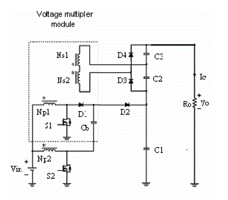
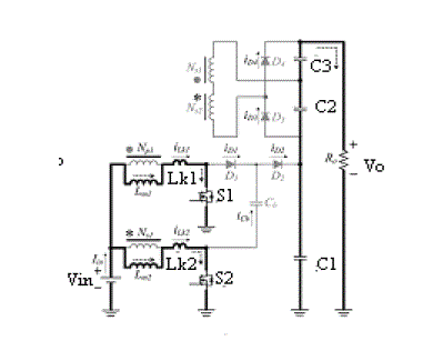
| The Fig 1 shows the circuit configuration of the proposed an asymmetrical interleaved converter with voltage multiplier cell. The voltage multiplier module of the proposed converter is composed of coupled inductor, the conventional boost converter and a voltage-lift capacitor[20]. This capacitor offers an extra voltage conversion ratio. The leakage energy of the coupled inductor is recycled to the output capacitors the turns ratio of coupled inductors can be designed to enlarge voltage gain. The number of multiplier can be adjusted to get a desired duty ratio; a higher boost rate is easily obtained from the voltage multiplier [13]. The coupling coefficient of the coupled inductor is denoted by “.” And “*”.The equivalent circuit of coupled inductor include the magnetizing inductor Lm, Lk. This proposed converter consist of the dc input voltage Vin, two power switch S1 and S2, four diodes D1, D2, D3, D4 and four capacitors C1, C2, C3, Cb. Primary winding of the couple inductor turn is Np1 and the secondary winding of the turn is Ns2. |
| The Proposed system advantages are |
| 1) The converter is characterized by a low input current ripple and low conduction losses, making it suitable for highpower applications; |
| 2) The converter achieves the high step-up voltage gain that renewable energy system. |
| 3) Leakage energy is reuse and sent to the output terminal, and ease large voltage spikes on the main switch |
| 4) The main switch voltage stress of the converter is considerably lower than that of the output. |
PRINCIPLE OF OPERATION
|
| A voltage multiplier is an electrical circuit that converts electrical power from a lower voltage to a higher voltage. Module, which is stacked on a boost converter to form an asymmetrical interleaved structure [14]. Primary windings of the coupled inductors with np turnsare employed to decrease input current ripple, and secondarywindings of the coupled inductors with ns turns are connected in series to extend voltage gain. The turns ratios of the coupled inductors are the same. |
| The proposed converter operates in continuous conduction mode (CCM), and the duty cycles of the power switches during steady operation are interleaved with a 180âÃâæ phase shift; the duty cycles are greater than 0.5 conventional interleaved boost converter [15]. Interleaved structure is employed in the input side to reduce the input current ripple and improve the power level. |
| The voltage multiplier cell is placed in the output side to achieve a high step up voltage gain and simplify the circuit structure. Moreover, the switch voltage stress is reduced as the turns ratio of the coupled inductors increases. The output voltage is changed as load shift and the detected feedback signal is processed via proportional-integral controller, and the internal comparator generates interleaved PWM with a 180° phase shift.The key steady waveforms in one switching period of the proposed converter contain six modes |
MODES OF OPERATIONS
|
| Mode1 [t0, t1 ] |
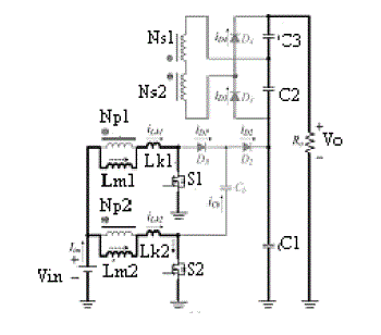
| At t=t0 , the S1 and S2 both switches areturned on ,all the diodes are get reversed-biased . The magnetizing inductors Lm1 , Lm2 and the leakage inductorsLk1, Lk2 are linearly charged by the input voltage sourceVin ,the circuit is shown in fig 2.(a) |
| Mode 2 [t 1 , t 2 ] |
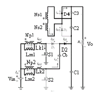
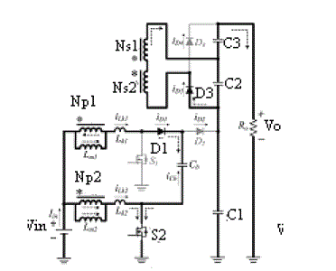
| At t= t1, the power switch s2 is switchedoff, thereby diodes D2 and d4 is turned on. The energy stored in themagnetizing inductor Lm2 is transferred to the secondary side, this charging the output filter capacitor C3. The inputvoltage source, magnetizing inductor Lm2 , leakage inductorLk2 , and voltage-lift capacitor Cb release energy to the outputfilter capacitor c1 through diode D2 , thereby extending the voltageon C1.The circuit is shown in fig 2.(b). |
| Mode 3 [t 2 , t 3 ] |
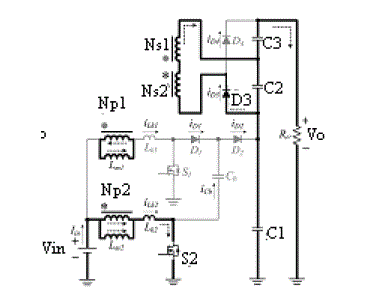
| At t=t2, the total energy of leakage inductor Lk2 has beencompletely released to the output filter capacitor C1 , the diode D2 automatically switchesoff so there is no reverse recovery problem in the diode. Magnetizing inductor Lm2 transfers energy to the secondary side chargingthe output filter capacitor C3 through the diode D4 until t3. The circuit is shown in fig.2(c). |
| Mode 4 [t 3 , t 4 ] |
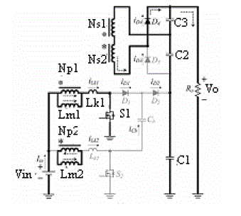
| At t= t3, the power switch S2 is switchedon and all the diodes are reversed biased. The magnetic inductance and leakage inductance gets linearly charged by the input voltage Vin. The circuit is shown in fig 2.(d). This mode 4 is similar to mode 1. |
| Mode 5 [t 4, t 5] |
| At t=t4, the power switch S1 is switchedoff, which turns on diodes D1 and D3.The energy stored in magnetizing magnetizing inductor Lm1 is transferredto the secondary sidecharging the output filter capacitor C2. The input voltage source and magnetizing inductor Lm1 release energy to voltage-lift capacitor Cb via diode D1, which stores extra energy in Cb. This mode of operation is shown in fig 2. (e) |
| Mode 6 [t 5, t 0 ] |
| At t = t5, the total energy of leakage inductor Lk1 has been completely released to voltage-lift capacitor Cb, so the diode D1 is automatically turned off . Magnetizing inductor Lm1 transfers energy to the secondary side charging the output filter capacitor C2 via diode D3 until t0. |
SIMULATION RESULT AND DISCUSSION
|
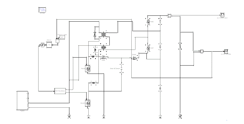
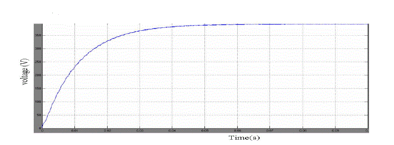
| The circuits are simulated in MATLAB software. The circuit simulation of high step up converter and the output waveforms are shown in fig 3and fig 4 respectively .In the proposed high step up converter 380-V output s obtained for 40-V input. The simulation result of the proposed converter is shown in fig 4. |
| The proposed high step up converter function is based on the components selection and coupled inductor design .The values of the primary leakage inductors of the coupled inductors are set as close as possible for current sharing performance.When the duty cycle ratio is 0.6 , the voltage gain is 10 at a turns ratio n = 1, but the gain reaches 10 at a turns ratio n = 5. The efficiency of the proposed converter is 96.8% at Po=400W at maximum output power the conversion efficiency of the converter about 96.1%. The performance of the proposed converter is compared with the other interleaved converters introduced in [13] and [14] as shown Table 2. |
CONCLUSION
|
| This work done has presented the topological principles, and simulation results for a proposed converter. The proposed converter has been successfully implemented in an efficiently high step-up conversion without an extreme duty ratio and a number of turns ratios through the voltage multiplier module and voltage clamp feature. The interleaved PWM scheme reduces the current that pass through each power switch and constrained the input current ripple by approximately 6%. The experimental results indicate that leakage energy is recycled through capacitor Cb to the output terminal.The voltage stresses over the power switches are restricted much lower than the output voltage (380V). These switches, conducted to low voltage rated and low on-state resistance MOSFET, can be selected. From the aforementioned workdone, the major challenges are as follows: |
| 1) how to extend the voltage gain and how to avoid the extreme duty cycle to reduce the current ripple; |
| 2) how to reduce the switch voltage to make low-voltage MOSFETs available to re duce the power device cost and conduction losses; |
| 3) how to realize the soft switching performance to reduce the switching losses; |
| 4) how to alleviate the output diode reverse recovery problem to reduce the reverse recovery losses. |
Tables at a glance
|
 |
 |
| Table 1 |
Table 2 |
|
Figures at a glance
|
 |
 |
 |
 |
 |
| Figure 1 |
Figure 2a |
Figure 2b |
Figure 2c |
Figure 2d |
 |
 |
 |
 |
| Figure 2e |
Figure 2f |
Figure 3 |
Figure 4 |
|
References
|
- C. Hua, J. Lin, and C. Shen, “Implementation of a DSP-controlled photovoltaic system with peak power tracking,” IEEE Trans. Ind.Electron, vol. 45, no. 1, pp. 99–107, Feb. 1998.
- J. M. Carrasco, L. G. Franquelo, J. T. Bialasiewicz, E. Galvan, R. C. P. Guisado, M. A. M Prats, J. I. Leon, and N. Moreno-Alfonso,“Power-electronic systems for the grid integration of renewable energy sources: A survey,” IEEE Trans. Ind. Electron., vol. 53, no. 4, pp.1002–1016, Jun. 2006.
- J. T. Bialasiewicz, “Renewable energy systems with photovoltaic power generators: Operation and modeling,” IEEE Trans. Ind.Electron., vol. 55, no. 7, pp. 2752–2758, Jul. 2008.
- Y. Xiong, X. Cheng, Z. J. Shen, C. Mi, H.Wu, and V. K. Garg, “Prognostic and warning system for power-electronic modules in electric,hybrid electric, and fuel-cell vehicles,” IEEE Trans. Ind. Electron., vol. 55, no. 6, pp. 2268–2276, Jun. 2008.
- F. S. Pai, “An improved utility interface for micro-turbine generation system with stand-alone operation capabilities,” IEEE Trans. Ind.Electron, vol. 53, no. 5, pp. 1529–1537, Oct. 2006.
- H. Tao, J. L. Duarte, and M. A. M. Hendrix, “Line-interactive UPS using a fuel cell as the primary source,” IEEE Trans. Ind. Electron., vol.55, no. 8, pp. 3012–3021, Aug. 2008.
- Z. Jiang and R. A. Dougal, “A compact digitally controlled fuel cell/battery hybrid power source,” IEEE Trans. Ind. Electron., vol. 53, no.4, pp. 1094–1104, Jun. 2006.
- G. K .Andersen, C.Klumpner, S. B. Kjaer, and F. Blaabjerg, “A newgreen power inverter for fuel cells,” in Proc. IEEE 33rd Annu. PowerElectron. Spec. Conf., 2002, pp. 727–733.
- H. Ghoddami and A. Yazdani, “A single-stage three-phase photovoltaic system with enhanced maximum power point tracking capabilityand increased power rating,” IEEE Trans. Power Del., vol. 26, no. 2, pp. 1017– 1029, Apr. 2011.
- B. Yang, W. Li, Y. Zhao, and X. He, “Design and analysis of a gridconnectedphotovoltaic power system,” IEEE Trans. Power Electron,vol. 25, no. 4, pp. 992–1000, Apr. 2010.
- W. Li and X. He, “Review of Nonisolated high-step-up DC/DC converters in photovoltaic grid-connected applications,” IEEE Trans. Ind.Electron., vol. 58, no. 4, pp. 1239–1250, Apr. 2011.
- Y. T. Jang andM. M. Jovanovic, “Interleaved boost converter with intrinsic voltage-doublers characteristic for universal-line PFC frontend,” IEEE Trans. Power Electron., vol. 22, no. 4, pp. 1394–1401, Jul. 2007.
- W. Li, Y. Zhao, J. Wu, and X. He, “Interleavedhigh step-up converter with winding-cross-coupled inductors and voltage multiplier cells,”IEEETrans. Power Electron., vol. 27, no. 1, pp. 133–143, Jan. 2012
- C. M. Lai, C. T. Pan, and M. C. Cheng, “High-efficiency modular highstep-up interleaved boost converter for DC-micro gridapplications,” IEEETrans. Ind. Electron., vol. 48, no. 1, pp. 161–171, Jan/Feb. 2012.
- J. W. Baek,M. H. Ryoo, T. J. Kim, D. W. Yoo, and J. S. Kim, “High boost converter using voltage multiplier,” in Proc. 31st Annu. Conf.IEEE Ind. Electron .Soc., May 2005,pp.567-572.IEEE Ind.
|