Keywords
|
| Flash ADC, Preamplifier based latch Comparator, Low power consumption. |
INTRODUCTION
|
| Analog to digital converters plays a prominent role to interact with the real world. Flash ADC is the fastest ADC in comparison with other ADC architectures. Flash ADC is the best choice in high speed low resolution applications. It is highly used in high data rate links, high speed instrumentation, radar, digital oscilloscopes and optical communications. Since flash ADC is operating in parallel conversion method, maximum operating frequency in the range of gigahertz is possible. |
| In this paper we are designing a low power, high speed comparator. Here we are combining two recently published research papers to achieve the low power and high speed in ADC. In [2] a Low power flash ADC with 6 bit resolution uses inverter based comparator which consumes a less power of 300 μW at a sampling rate of 50MS/s. In [3] a high speed flash ADC with 6 bit resolution uses differential clocked comparator architecture. Even though the sampling speed is 1GS/s, the comparator block alone consumes 2mW of power. The present work collaborates the above explained two papers in order to fill the gap by proposing a 6 bit flash ADC for high speed applications (up to 5 GS/s) and slightly higher power compared to the inverter based ADC. The proposed ADC employs a modified version of the comparator block presented in [3] to achieve low power and high speed of operation. |
LITERATURE SURVEY
|
| R Komar, et.al, proposed “A 0.5V 300μw 50MS/s 180nm 6-bit flash adc using inverter based comparators”. This paper presents a 0.5 V, 50 MS/s, 6 bit Flash ADC designed using 180 nm CMOS technology. To reduce the silicon area and power requirement, an inverter based comparator is used in the design. Low threshold MOSFETs are used for the ultra low voltage operation. A simple clock delaying technique and back to back inverters in the comparator have been used to increase the power efficiency and speed of operation. A fat tree encoder design is used for digitizing comparator outputs. The measured SNDR at input frequency of 5.1 MHz is 31 dB. The measured maximum INL and DNL for a ramp input are 0.375 LSB and 0.025 LSB, respectively. The design consumes a very low power of 0.3mW. |
| S. Sheikhaei, et.al, proposed “A 0.35 μm cmos comparator circuit for high-speed adc applications”. A high-speed differential clocked comparator circuit is presented. The comparator consists of a preamplifier and a latch stage followed by a dynamic latch that operates as an output sampler. The output sampler circuit consists of a full transmission gate (TG) and two inverters. The use of this sampling stage results in a reduction in the power consumption of this high-speed comparator. Simulations show that charge injection of the TG adds constructively to the sampled signal value, therefore amplifying the sampled signal with a modest gain of 1.15. Combined with the high gain of the inverters, the sampled signals are amplified toward the rail voltages. This comparator is designed and fabricated in a 0.35μm standard digital CMOS technology. Measurement results show a sampling frequency of 1GHz with 16mV resolution for a 1V input signal range and 2mW power consumption from a 3.3V supply. |
| Kirankumar Lad and M S Bhat, designed “A 1-V 1-GS/s 6-bit low power flash ADC in 90 nm CMOS with 15.75mW power consumption”. A 1-V 1-GS/s 6-bit low power flash ADC in 90 nm CMOS technology is presented. Proposed Flash ADC consists of reference generator, comparator array, 1-out-of N code generator, Fat tree encoder and output D-latches. This Flash ADC achieves 5.76 ENOB at Nyquist input frequency without calibration. The measured peak INL and DNL are 0.08LSB and 0.1LSB, respectively. The proposed ADC consumes 15.75 mW from 1V supply and yielding an energy efficiency of 0.291 pJ/conv while operating at 1 GS/s. |
| Timmy Sundstrom and Atila Alvandpour, proposed “A 2.5-GS/s 30-mW 4-bit Flash ADC in 90nm CMOS”. A 2.5 GS/s flash ADC, fabricated in 90nm CMOS, avoids traditional power, speed and accuracy trade-offs by using comparator redundancy with power-gating capabilities. Redundancy removes the need to control comparator offsets, allowing the large process-variation induced mismatch of small devices in nanometer technologies. This enables the use of small sized, ultra-low-power comparators. Measurement results show that the ADC dissipates 30 mW at 1.2 V. With 63 gate-able comparators, the ADC achieves 4.0 effective number of bits. |
FLASH ADC DESIGN
|
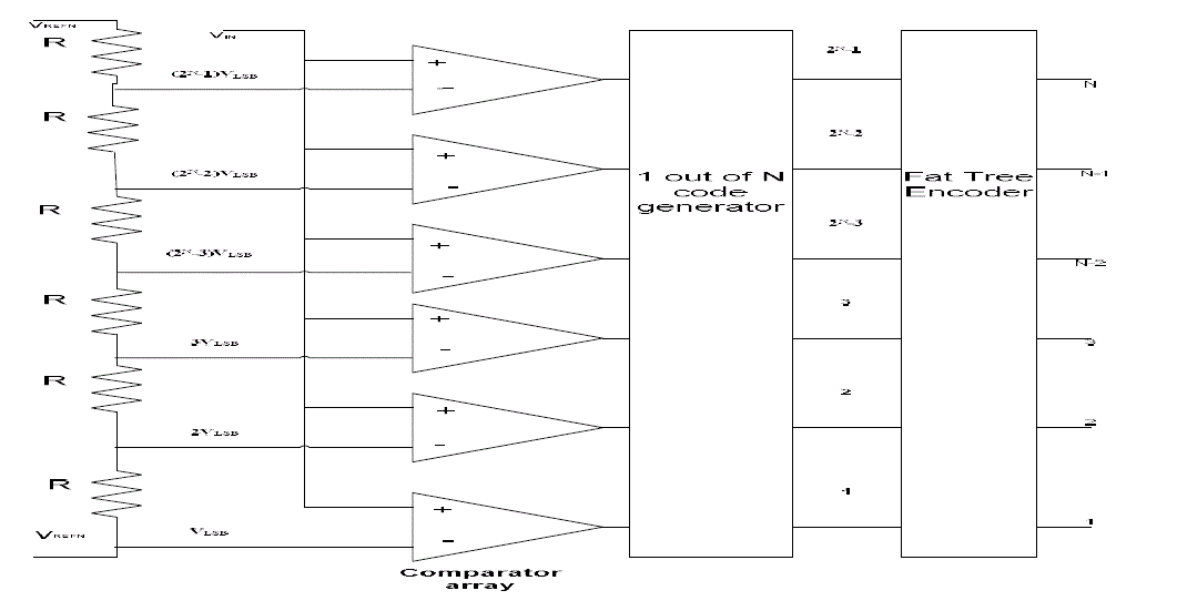
| The proposed ADC block diagram is shown in Fig 1. Individual blocks are briefly explained below. |
A. Reference Voltage Generator
|
| It can be seen from the Fig 1, that 2N-1 comparators are required for an "N" bit converter. The resistor ladder network is formed by 2N equal resistors, which is used to generate the reference voltages for each of the comparator. The reference voltage for each comparator is 1 least significant bit (LSB) less than the reference voltage for the comparator immediately above it. In this work, the input dynamic range is fixed as 0.4 V peak - to- peak and the reference voltage ranges from 0.2 V to 0.6V with a step size of 6.25 mV (LSB). |
B. Voltage Comparator
|
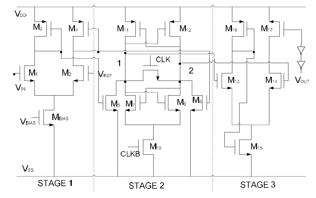
| The circuit diagram of the proposed voltage comparator is shown in Fig 2. This comparator has been divided into three sections: a preamplifier stage, a decision circuit (latch) and a post amplifier stage [4]. The working of each section is described below |
C. Preamplifier
|
| The stage-1 of proposed comparator shown in Fig 2 is working as a preamplifier. The pre-amplifier amplifies the difference between input voltage and the reference voltage generated by the resistive ladder of the ADC. The preamplifier is a circuit which is used to amplify the signal so that it can easily drive the load. In most latched comparator design of pre-amplifiers are also used to avoid the kickback effect from the latch and input referred offset. |
| Here M1 and M2 form the input differential pair. Input voltage VIN is applied to M1and reference voltage VREF is applied to the M2.Preamplifier compares the voltage difference between M1 and M2 and amplifies it.M3 and M4 are the diode connected PMOS pair which acts as a load. Preamplifier in this circuit has to continuously track the input signal because sample and hold circuit is not used in this flash ADC frontend. There is a error (or bubble) code due to the large difference in delays across different preamplifiers. The output of the Preamplifier is fed to the latch staged MOSFETs M5 and M6. |
D. Latch
|
| The stage-2 of proposed comparator shown in Fig 2 works as a Latch. Basic function of the latch in any circuit is as a memory element, which is used to store the value. Latch is defined as the memory unit that stores the charge on the gate capacitance of the inverter. The Latch stage consists of a cross coupled pair of PMOS and NMOS transistors. The Latch works in two phases. One is when the CLK is LOW and the other is when the CLK is high. |
| When CLK is LOW and CLKB is HIGH the Latch is in reset phase. During reset phase M5, M6, M7, M8, M10 are in ON state, M9 is in OFF state. VSS will be the voltages present at the nodes 1 and 2, which makes M11 and M12 ON. Therefore the output voltages are at the midpoint of the rails i.e., the preamplifier translates the voltage difference between the inputs of the differential pair into an unbalanced state in the latch stage. When CLK is HIGH and CLKB is LOW the Latch is in evaluation phase. During evaluation phase M5, M6, M7, M8, M9 are in ON state, M10 is in OFF state. At present the voltage at node 1 and 2 is VDD which will make to turn OFF M11 and M12. |
E. Postamplifier
|
| The stage-3 of proposed comparator shown in Fig 2 works as a Postamplifier. In the Postamplifier M15, M16, M17 are self biased, they are always ON by default. The working of the post amplifier depends on the working of the Latch. When the CLK is LOW and CLKB is HIGH, M11 and M12 are in the ON state in the Latch stage. This M11 and M12 will turn ON the M13 and M14 of the postamplifier. Now the Voltage at the output of the postamplifier is VSS (i.e., LOW). When the CLK is HIGH and CLKB is LOW, the voltage at node 1 and 2 is VDD which will turn OFF M11 and M12 MOSFETs. This M11 and M12 will turn OFF the M13 and M14 of the postamplifier. Now the Voltage at the output of the postamplifier is VDD (i.e., HIGH). The back to back inverters are used to remove the glitches present at the output of the buffer and also to provide an additional gain. Output of the postamplifier stage forms a thermometer code and this thermometer code is converted into a 1-outof-N code generator. |
F. 1- out of N code generator, Fat tree encoder and D-latch
|
| A Bank of NOT and AND is used in order to convert the thermometer code into a 1-outof-N code generator. This bank of NOT-AND gates are realized using NOT and NOR gates. This 1 out of-N code is fed to a fat tree encoder, which converts it into a binary code. The fat tree encoder performs better than ROM encoder in terms of speed and power in case of a 6-bit flash ADC and it also consumes less silicon area [5]. The OR gates of fat tree encoder are realized using NAND and NOR gates. The six output binary bits from the fat tree encoder are latched using a positive edge D-latch, which gives synchronized output and acts as an output register. |
| DESIGN VALUES: VDD=0.8V, VREF=0.4V, KP nmos=100μA/V2, KPpmos=40μA/V2, (W/L) nmos= 11.45, (W/L)pmos= 22.85 |
SIMULATION RESULTS
|
| The proposed Low power comparator is implemented in 90 nm CMOS technology and simulated using H Spice and LT Spice Tool. The supply voltage and reference voltage used are 0.8 V and 0.4 V, respectively. The sampling rate of this ADC is 1.2 GHz. |
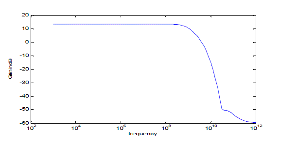
| The frequency response at 90nm is shown in Fig 3 which has a gain of 13.59dB. This scheme at 90nm consumes a very low power of 7.67mW, the power consumption is almost reduced to 50% of the previous referred approaches. Comparison of this work with recently reported high sampling speed ADCs is given in Table 1. From Table 1, it can be observed that the present work has half the power consumption as compared to the wok of [1]. The ADC works at a sampling speed of 1.2 GS/s with a supply voltage of 0.8v. Further, this ADC consumes lesser power; it can be used in high speed low power ADC applications. |
CONCLUSION
|
| In this paper, the design and the simulation results of 0.8-V 1.2-GS/s 6-bit low power Flash ADC are represented. This scheme consumes a very less power of 7.67mW, which consumes a less power of about 50% of the previous referred approaches. This architecture can be extended to high speed applications because the comparator used in this ADC can work up to 5 GS/s. As the ADC has high input bandwidth, low power consumption and high linearity, this ADC is most suitable for high speed communication applications up to 1.2 GS/s. |
Tables at a glance
|
 |
| Table 1 |
|
Figures at a glance
|
 |
 |
 |
| Figure 1 |
Figure 2 |
Figure 3 |
|
References
|
- Kirankumar Lad and M S Bhat âÃâ¬Ãâ¢A 1-V 1-GS/s 6-bit Low-Power Flash ADC in 90-nm CMOS with 15.75 mW Power Consumption,âÃâ¬Ãâ inComputer Communication and Informatics (ICCCI), 2013 International Conference on. IEEE, 2013.
- R.Komar, M. Bhat, and T. Laxminidhi, âÃâ¬Ãâ¢A 0.5 v 300μw 50ms/s 180nm 6bit flash adc using inverter based comparators,âÃâ¬Ãâ in Advances in Engineering, Science and Management (ICAESM), 2012 International Conference on. IEEE, 2012, pp. 331–335.
- S.Sheikhaei, S. Mirabbasi, and A. Ivanov, âÃâ¬Ãâ¢A 0.35 μmcmos com-parator circuit for high-speed adc applications,âÃâ¬Ãâ in ISCAS-2005. IEEE International Symposium on Circuits and Systems. IEEE, 2005, pp. 6134–6137.
- A.Venes and R. van-de Plassche, âÃâ¬Ãâ¢An 80-mhz, 80-mw, 8-b cmos folding a/d converter with distributed track-and-hold preprocessing,âÃâ¬Ãâ IEEE Journal of Solid-State Circuits, vol. 31, no. 12, pp. 1846–1853, 1996.
- R.Baker, CMOS Mixed Signal Circuit Design. John Wiley & Sons, 2008.
- D. Lee, J. Yoo, K. Choi, and J. Ghaznavi, âÃâ¬Ãâ¢Fat tree encoder design for ultra-high speed flash a/d converters,âÃâ¬Ãâ in MWSCAS2002. The 2002 45th Midwest Symposium on Circuits and Systems, vol. 2. IEEE, 2002, pp. II–87.
- P E Allen, D R Holberg, CMOS Analog Circuit Design, second Edition, Oxford university press.
- A S Sedra, K C Smith, Microelectronic Circuits, fifth Edition, Oxford university press, 2004.
- C. Sandner, M. Clara, A. Santner, T. Hartig, and F. Kuttner, âÃâ¬Ãâ¢A 6-bit 1.2-gs/s low-power flash-adc in 0.13-μm digital cmos,âÃâ¬Ãâ Solid-State Circuits, IEEE Journal of, vol. 40, no. 7, pp. 1499–1505, 2005.
- S. Park, Y. Palaskas, A. Ravi, R. Bishop, and M. Flynn, âÃâ¬Ãâ¢A 3.5 gs/s 5-b flash adc in 90 nm cmos,âÃâ¬Ãâ in Custom Integrated Circuits Conference, 2006. CICC’06. IEEE. IEEE, 2006, pp. 489–492.
- T. Sundstrom and A. Alvandpour, âÃâ¬Ãâ¢A 2.5-gs/s 30-mw 4-bit flash adc in 90nm cmos,âÃâ¬Ãâ in NORCHIP, 2008. IEEE, 2008, pp. 264–267.
|