Keywords
|
| Cognitive Radio, Spectrum Sensing, Efficient Communication, System Security. |
INTRODUCTION
|
| The first semiconductor chips held one transistor each. Subsequent advances added more and more transistors, and, as a consequence, more individual functions or systems were integrated over time. The first integrated circuits held only a few devices, perhaps as many as ten diodes, transistors, resistors and capacitors, making it possible to fabricate one or more logic gates on a single device. Now known retrospectively as "small-scale integration" (SSI), improvements in technique led to devices with hundreds of logic gates, known as large-scale integration (LSI), i.e. systems with at least a thousand logic gates. Current technology has moved far past this mark and today's microprocessors have many millions of gates and hundreds of millions of individual transistors. At one time, there was an effort to name and calibrate various levels of large-scale integration above VLSI. Terms like Ultra-large-scale Integration (ULSI) were used. But the huge number of gates and transistors available on common devices has rendered such fine distinctions moot. Terms suggesting greater than VLSI levels of integration are no longer in widespread use. Even VLSI is now somewhat quaint, given the common assumption that all microprocessors are VLSI or better. |
| As of early 2008, billion-transistor processors are commercially available, an example of which is Intel's Montecito Itanium chip. This is expected to become more commonplace as semiconductor fabrication moves from the current generation of 65 nm processes to the next 45 nm generations (while experiencing new challenges such as increased variation across process corners). Another notable example is NVIDIA’s 280 series GPU. This microprocessor is unique in the fact that its 1.4 Billion transistor count, capable of a teraflop of performance, is almost entirely dedicated to logic (Itanium's transistor count is largely due to the 24MB L3 cache). Current designs, as opposed to the earliest devices, use extensive design automation and automated logic synthesis to lay out the transistors, enabling higher levels of complexity in the resulting logic functionality. Certain high-performance logic blocks like the SRAM cell, however, are still designed by hand to ensure the highest efficiency (sometimes by bending or breaking established design rules to obtain the last bit of performance by trading stability). |
| While we will concentrate on integrated circuits , the properties of integrated circuits-what we can and cannot efficiently put in an integrated circuit-largely determine the architecture of the entire system. Integrated circuits improve system characteristics in several critical ways. ICs have three key advantages over digital circuits built from discrete components. Integrated circuits are much smaller-both transistors and wires are shrunk to micrometer sizes, compared to the millimeter or centimeter scales of discrete components. Small size leads to advantages in speed and power consumption, since smaller components have smaller parasitic resistances, capacitances, and inductances. |
| Signals can be switched between logic 0 and logic 1 much quicker within a chip than they can between chips. Communication within a chip can occur hundreds of times faster than communication between chips on a printed circuit board. The high speed of circuits on-chip is due to their small size-smaller components and wires have smaller parasitic capacitances to slow down the signal. Logic operations within a chip also take much less power. Once again, lower power consumption is largely due to the small size of circuits on the chip-smaller parasitic capacitances and resistances require less power to drive them. |
| These advantages of integrated circuits translate into advantages at the system level. Smaller physical size. Smallness is often an advantage in itself-consider portable televisions or handheld cellular telephones. Lower power consumption. Replacing a handful of standard parts with a single chip reduces total power consumption. Reducing power consumption has a ripple effect on the rest of the system: a smaller, cheaper power supply can be used; since less power consumption means less heat, a fan may no longer be necessary; a simpler cabinet with less shielding for electromagnetic shielding may be feasible, too. Reduced cost. Reducing the number of components, the power supply requirements, cabinet costs, and so on, will inevitably reduce system cost. The ripple effect of integration is such that the cost of a system built from custom ICs can be less, even though the individual ICs cost more than the standard parts they replace. Understanding why integrated circuit technology has such profound influence on the design of digital systems requires understanding both the technology of IC manufacturing and the economics of ICs and digital systems. |
| In this paper the design of NAND flash memory is summarized and results pertaining to the simulation and synthesisation are presented. |
DESIGN CONSIDERATION OF NAND FLASH MEMORY
|
| The design of NAND FLASH CONTROLLER incorporates various design blocks like Arithmetic Logic Unit (ALU), Accumulator, Program Counter (PC), Instruction Register (IR), Memory, Control Unit (CU), and additional logic. |
| the design incorporates some the issues like handling 32 bit data ,28 bit address, using fixed instruction format of length 32 bit, size of opcode is of 4 bit, handling 15 instructions, has 256 memory locations, 32-bit registers (IR,ACC), Implements 2-staged pipelining i.e overlap of fetch and execute cycles, has two addressing modes ,Register addressing and memory addressing modes, no interrupts and No conditional branches, data that it handles is unsigned integer type. |
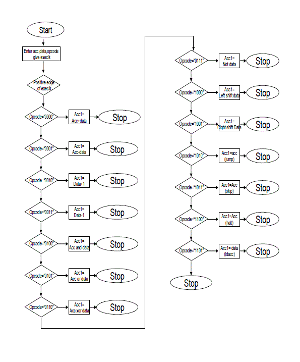
| The ALU performs both arithmetic and logical operations and as well as control of transfer instructions. It takes data and acc as inputs to generate output according to the opcode. An execlk is given as input for synchronization and the output is available at positive edge of the execlk. It performs arithmetic and logic instructions directly and control of transfer instructions are performed with the help of control and logic decoder. |
| The result of an Alu operation is always stored in accumulator at some specified time based on the control logic instruction and also the execlk. This output is again fed to Alu as input. If Reset =0, the output of accumulator is cleared to zero. When reset is high and load accumulator signal is set high, the output of the ALU is loaded in to the accumulator at the negative edge of the execlock. |
| A buffer is used for writing data in to memory. When it is required to write data in to the memory, then necessary control signals are generated at the buffer. Buffer is used for achieving bi-directional operation of the data bus. |
| The flow chart describing the implementation and synthesis and operation part is given as follows. |
RESULTS
|
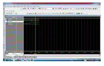
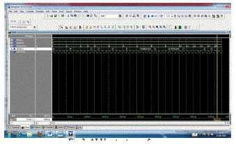
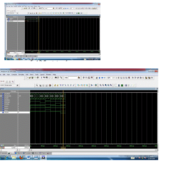
| The results pertaining to various blocks of the NAND flash memory implementation are presented in this section. The out put plots referring the corresponding input and output are given in this section. |
CONCLUSION
|
| It is observed that the NAND FLASH CONTROLLER based system is simulated using VHDL. The overall system is simulated and synthesized. After synthesizing the system we could get a statistical data about the number of inputoutput buffers, the number of registers, number of flip-flops and latches were used .The modules simulated are Accumulator, Buffer, , Instruction Register, Multiplexer, Program Counter, Control Logic Decoder, Arithmetic Logic Unit and the overall system. Few instructions were executed and their timing sequences were analyzed. It shows that the different operations of the instruction including the decoding and execution comes in the overall system. Therefore we conclude that the behavior shows, the system is working as NAND FLASH CONTROLLER as instruction will be executed within a single clock cycle. |
Figures at a glance
|
 |
 |
 |
 |
| Figure 1 |
Figure 2 |
Figure 3 |
Figure 4 |
|
References
|
- Shawn Kung, “Native PCIs SSD Controllers Next Generation Enterprise Architecture for Scalable I/O Performance”, White Paper MarvellJan-2012.
- Yang Ou, Nong Xiao, “A Scalable Multi-channel Parallel NAND Flash Memory Controller Architecture”, 6th Annual IEEE ChinagridConference, Page 48-53, 2011.
- Yu Cai, Haratsch, “FPGA Based Solid State Drive Prototyping Platform”, 19th IEEE Annual International Symposium on Field- Programmable Custom Computing Machines (FCCM), Page 101-104, 2011.
- Yu Chi, Erich F. Haratsch, Mark McCatney and Ken Mai “FPGA-Based Solid State Drive Prototyping Platform,” In IEEE InternationalSymposium on Field Programmable Custom Computing Machines 2011.
- Yang Ou, Nong Xiao and Mingche Lai “A Scalable Multi-channel Parallel NAND Flash Memory Controller Architecture,” Sixth AnnualChinaGrid Conference 2011.
- International Technology Roadmap for Semiconductor, 2007.
- Micron Technology, Boise, Idaho. Technical Note TN-29-17 “Design and Use Considerations for NAND FlashMemory,” 2006.
- Altera Corporation, Stratix data isheet, May 2003.
|