Keywords
|
| Small-signal amplifiers, Darlington amplifiers, Common Source JFET amplifiers |
INTRODUCTION
|
| One of the important concepts in electronics is the process of amplification through Darlington pair which is considered to be a prominent configuration due to its wide range of application [1]-[5]. The flexible application-range of this vital configuration is extended from small-signal amplifiers to power amplifier circuits [1]-[5]. However, a major drawback is associated with small-signal Darlington pair amplifier i.e. at higher frequencies its response becomes poor than that of a single transistor amplifier [3]-[5]. Various attempts have been made to defeat this problem by proposing different modifications in Darlington’s composite unit as well as in respective amplifier circuits [6]-[10]. These efforts include the use of Field Effect Transistors in paired unit [11]-[13], experimentation with Triple Darlington’s topology [5], [14]-[16] or the inclusion of some extra biasing resistances in respective circuits [3]-[4], [12], [15]-[16]. However, use of dissimilar active devices or hybrid combination of active devices in Darlington’s topology (such as Darlington’s unit with BJT and FET or BJT and MOSFET etc.) is still an area of electronic circuit designers to work with [11]-[13], [17]. |
| If two identical NPN or PNP transistors are coupled as to form a CC/CE Darlington pair, the current gain of this composite unit of transistors is theoretically considered to be identical to the product of current gains of the individual transistors while the voltage gain climbs down to a considerable limit [3]-[5], [9], [15]-[16]. However, the input resistance of Darlington pair amplifier is much higher and output resistance is lower than that of a single-stage Emitter Follower [1], [3]-[5], [9], [15]-[16]. Similarly, if two identical FETs are coupled as to form a common source JFET Darlington pair amplifier, the input impedance of this configuration is found much higher than that of a BJT amplifier with generally low voltage gain (with inverted output waveform) and improved band width [18]. |
| Though the qualitative properties of BJTs and FETs are entirely different [1]-[2], [11], [19], nevertheless in the present manuscript, authors have proposed two novel circuit models of small-signal amplifiers using hybrid combination of BJT, JFET and BJT in Triple Darlington topology. The proposed amplifiers are well suited for the stages requiring high voltage with moderate range bandwidth and current gain. |
| The present paper is described in four sections. Section I gives the Introduction of the Darlington’s topologies and the idea behind proposed circuits. Section II describes the configuration and component details of the proposed amplifiers. Section III contains the observational details and related discussions whereas the last section IV concludes the proposed work followed by references. |
EXPERIMENTAL CIRCUITS
|
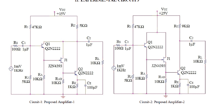
| The present study starts with a small-signal amplifier having compound unit of BJT-JFET-BJT in Triple Darlington topology [5], [10], [14]-[16]. Respective configuration and biasing idea is depicted as Circuit-1. However, the second proposed amplifier, depicted as Circuit-2, is obtained by implementing minor changes in the proposed amplifier Circuit-1. In this amplifier of Circuit-2, Q1 (NPN transistor Q2N2222) and J1 (N-channel JFET J2N4393) are directly connected with DC power supply and the value of RC is enhanced to 9KΩ. Assembly of Q1, J1 and Q2 in both the proposed amplifiers constitutes a Triple Darlington composite unit. |
| The proposed amplifier of Circuit-1 is biased with +15V whereas Circuit-2 is biased with +25V DC supply using potential divider network. Various biasing parameters and their respective values in context of the present study are listed in Table-I. |
| Respective observations related to the proposed circuits are carried out by feeding them with 1V AC input signal source. From this AC source, a small and distortion less signal of 1mV amplitude at 1 KHz frequency is drawn as input for amplification purpose. All the observations are furnished through ‘Student Version-9.2 PSpice Simulation Software’ [5], [10], [15]-[16], [20]. |
RESULTS AND DISCUSSIONS
|
| Amplifiers of Circuit-1 and 2 are found to provide fair and distortion-less results for 1-15mV and 1-4mV AC input signals respectively at the parameter values of Table-I. |
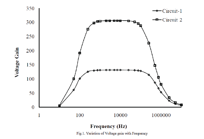
| Variation of voltage gain as a function of frequency for both the amplifiers is depicted in Fig.1. It is found that the proposed amplifier of Circuit-1 produces 131.388 maximum voltage gain, 60.248 maximum current gain and 440.671KHz bandwidth (with lower cut-off frequency fL=83.954Hz and upper cut-off frequency fH=440.755KHz), 13.975μA peak output current and 139.582 mV peak output voltage. However, the proposed amplifier of Circuit-2 produces 306.071 maximum voltage gain, 141.033 maximum current gain, 274.700KHz bandwidth (fL=124.470Hz and fH=274.825KHz), 30.812μA peak output current and 308.115 mV peak output voltage. Both the proposed amplifiers possess phase reversal in their output waveform. |
| Total Harmonic Distortion (THD) percentage is also calculated for both the proposed amplifiers for 10 significant harmonic terms using established formulae [1]-[2], [21]. For first proposed amplifier of Circuit-1, THD is found to be 0.84% whereas it is recorded as 1.21% for the proposed amplifier of Circuit-2. Mentioned values of THDs for both the proposed amplifeirs are falling in the permissible limit for small-signal amplifiers [1]-[2]. This clearly suggests that the modifications made in Circuit-1 to obtain the Proposed amplifier of Circuit-2 has almost doubled the corresponding values of maximum voltage and current gains (of Circuit-2) but on the cost of reduced frequency band and significantly enhanced THD. In addition, the proposed smallsignal amplifiers (of Circuit-1 and Circuit-2) having hybrid combination of BJT-FET-BJT in Triple Darlington topology produce improved voltage and current gains than that was designed by Tiwari et.al.[11] using compound unit of BJT-FET in Darlington pair configuration. |
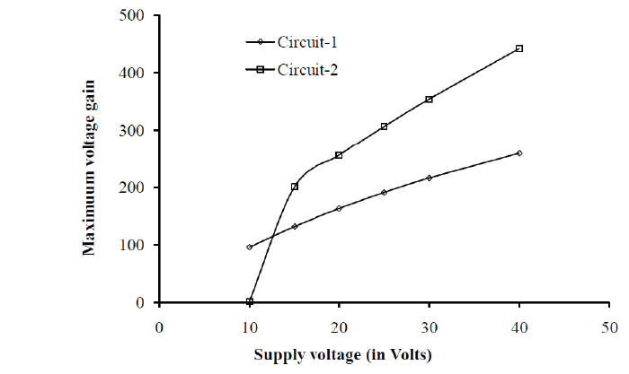
| Variation of maximum voltage gain with DC supply voltage is depicted in Fig.2. Figure suggests that the voltage gain for both the amplifiers rises nonlinearly at increasing values of VCC [10]-[11], [14]-[16]. This happens perhaps due the fact that on increasing biasing supply VCC, the saturation current of BJT driven Triple Darlington composite unit increases which in turn enhances the voltage and current across load resistance RL and hence the overall voltage gain of the respective amplifier circuits. The maximum permissible range of DC supply voltage for the distortion-less output corresponding to proposed amplifiers is 10-40V but at 10V the voltage gain for Circuit-2 is only 1.3376. |
| Variation of maximum voltage gain with DC supply voltage is depicted in Fig.2. Figure suggests that the voltage gain for both the amplifiers rises nonlinearly at increasing values of VCC [10]-[11], [14]-[16]. This happens perhaps due the fact that on increasing biasing supply VCC, the saturation current of BJT driven Triple Darlington composite unit increases which in turn enhances the voltage and current across load resistance RL and hence the overall voltage gain of the respective amplifier circuits. The maximum permissible range of DC supply voltage for the distortion-less output corresponding to proposed amplifiers is 10-40V but at 10V the voltage gain for Circuit-2 is only 1.3376. |
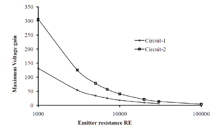
| Variation of maximum voltage gain as a function of emitter resistance RE is traced in Fig.3. Voltage gain decreases almost exponentially at increasing values of emitter resistance RE for both the proposed amplifiers (Circuit-1 and Circuit-2) [1]-[2], [14]-[16], [19], [21]. It is to be noted that the Circuit-1 produces considerable voltage gain in 1-30KΩ range of RE while this range for Circuit-2 is limited to 1-100KΩ. It is also observed that in absence of RE or the RC network of RE-CE, the voltage gain falls to an insignificant value with the disappearance of phase reversal in output waveforms. |
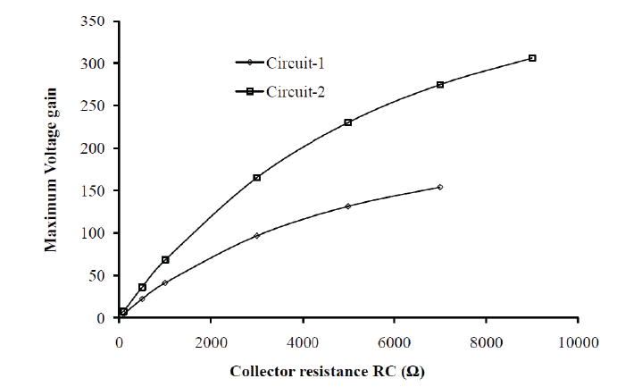
| Similar to RE, the maximum voltage gain of proposed amplifiers also depends highly on the collector resistance RC [1]-[2], [10], [14]-[16], [19], [21]. Its variation with RC is depicted in Fig.4. Voltage gain for both the amplifiers of Circuit-1 and Circuit-2 increases almost exponentially at increasing values of Collector resistance. However after 7KΩ of RC for Circuit-1 and 10KΩ for Circuit-2 amplifier voltage gain falls down below unity with distorted output. |
| In fact polarity of the composite unit of Darlington pair is determined by the driver device [21]. For example, a Darlington pair consisting NPN-BJT followed by N-Channel-JFET principally behaves like NPN-BJT driven Darlington unit. This is why the overall property of composite unit in proposed amplifiers (having BJT-JFET-BJT in Triple Darlington configuration) seems to be inclined more towards BJT (NPN) driven CE Darlington’s system. Therefore the effect of RE and RC on the voltage gain (Fig.3 and Fig.4) for proposed amplifiers can be explained on the basis of re equivalent model of RC coupled CE Transistor configuration. This model suggests that the overall voltage gain of the proposed circuits can be estimated by AV ≈ RC/RE. Hence increasing emitter resistance RE (at fixed RC), the overall voltage gain AV decreases whereas increasing RC (at fixed RE), the overall voltage gain AV increases almost exponentially. |
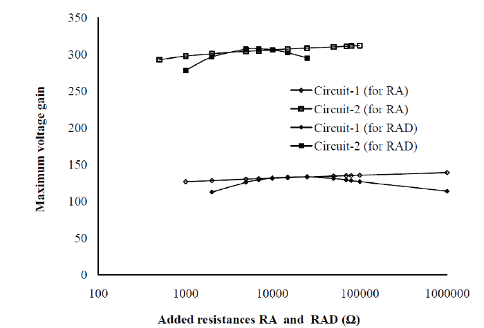
| Variation of Maximum voltage gain with added resistances RA and RAD is shown in Fig.5. It is noticed that increasing the value of RA, voltage gain increases leisurely for both the proposed amplifiers of Circuit-1 and Circuit-2. The Circuit-1 amplifier is found to produce distortion-less response in 500Ω-1MΩ range of RA whereas this range for Circuit-2 amplifier is 1KΩ- 100KΩ. After 1MΩ value of RA for Circuit-1 and 100KΩ for Circuit-2 amplifier the respective output waveforms shows distortion. It is also noticed that in absence of added resistance RA, voltage gain of both the amplifiers of Circuit-1 and Circuit-2 falls down to an insignificant value. |
| Similarly for increasing values of RAD, voltage gain corresponding to both the proposed amplifiers initially increases nonlinearly, thereafter, it acquires a peak value and then falls down to a limiting point. Maxim of the voltage gain corresponding to RAD for Circuit-1 amplifier is observed to be 133.155 at 25KΩ which falls down to 113.711 at 1MΩ. However for Circuit-2 the observed peak value of voltage gain is 307.474 at 7KΩ which climbs down to 294.833 at 25KΩ. Circuit-1 amplifier brings a distortion-less response in 2KΩ-1MΩ range of RAD while this range of RAD for Circuit-2 amplifier is 1KΩ-25KΩ. |
| It is observed that the voltage across added resistance RAD increases while current through it decreases to a considerable amount when the value of RAD is increased after a critical limit of 25KΩ for Circuit-1 and 7KΩ for Circuit-2. This in turn increases the forward biasing status of Base-Emitter junction of the transistor Q2. Due to this the current and voltage across RE considerably increases and causes a significant reduction in the voltage across load resistance RL and hence the overall voltage gain of the respective amplifiers. |
| It is also noticed that in absence of added resistance RAD, maximum voltage gain drops to an insignificant value 3.19 for amplifier of Circuit-1with distortion in output waveforms whereas for Circuit-2 amplifier it drops to 110.27 in absence of RAD with corresponding current gain 50.60 and 169.392KHz bandwidth (with fL=75.541Hz and fH=169.468KHz). However if RA and RAD both are simultaneously removed from the proposed circuits, voltage and current gains drop below unity and the output waveform clamps towards positive side of the reference axis. |
| During the qualitative analysis when biasing resistance R1 of the potential divider network of Circuit-1 amplifier was removed, Voltage gain of the respective circuit dropped to 61.019, Current gain to 24.532 whereas bandwidth increased to 1.628MHz (with fL=344.447KHz and fH=1.972MHz) with significant increase in THD. However, when R1 was removed from the amplifier of Circuit-2 its Voltage gain climbed down to 9.955, Current gain to 4.7201 whereas bandwidth increased to 6.210MHz (with fL=98.764KHz and fH=6.309MHz) with considerable rise in THD. On the other hand when R2 was removed from the configuration of the proposed circuits, the maximum voltage and current gains of respective amplifiers climbed down below unity with undistorted output waveforms. |
| Variation of maximum voltage gain with load resistance RL is also observed but not shown in form of figure. It is observed that voltage gain rises almost linearly to 100KΩ value of RL for both the amplifiers and then tends to acquire a saturation level. This rising and saturation tendency of the voltage gain with RL is well in accordance of the usual behaviour of small signal audio amplifiers [1]-[2], [14]-[16], [19]. |
CONCLUSIONS
|
| As a novel approach, a unique combination of BJT-FET-BJT is used in Triple Darlington configuration to explore two discrete circuits of small-signal amplifiers using RC coupling. At 1KHz input frequency, the proposed amplifier of Circuit-1 can effectively process small-signals ranging below 15mV in the frequency band of 83.954Hz to 440.755KHz whereas the proposed amplifier of Circuit-2 is able to process small-signals ranging below 4mV in 124.47Hz to 274.825KHz frequency band. |
| The proposed small-signal audio amplifiers are free from the problem of poor response of conventional small-signal Darlington pair or Triple Darlington amplifiers at higher order frequencies in the permissible frequency band. |
| With moderate range bandwidths, proposed amplifier of Circuit-1 generates only 0.84% harmonic distortion while the proposed amplifier of Circuit-2 generates 1.21% harmonic distortion but both the amplifiers simultaneously produces high voltage and current gains of considerable amount. High voltage as well as current gains of the proposed amplifiers logically set their power gain greater than unity. All these features together make these amplifiers fabulously unique in respective class of small signal audio amplifiers. |
| The proposed amplifiers show a considerable response for VCC, RE, RC and RL almost in the same way as is usually observed for small-signal RC coupled CE amplifiers. On the other hand the proposed amplifier of Circuit-1 provides an optimum performance in 1KΩ–1MΩ for additional biasing resistances RA whereas this range for RAD is 2KΩ–1MΩ. Similarly the optimum performance range for Circuit-2 amplifier corresponding to RA is 500Ω–100KΩ while that for RAD it is 1KΩ–25KΩ. |
Tables at a glance
|
 |
 |
| Table 1 |
Table 2 |
|
Figures at a glance
|
 |
 |
 |
| Figure 1 |
Figure 2 |
Figure 3 |
 |
 |
 |
| Figure 4 |
Figure 5 |
Figure 6 |
|
References
|
- R. L. Boylestad and L. Nashelsky, Electronic Devices and Circuit Theory, Pearson Education Asia, 3rd ed., p.263,307,600, 2002
- A. David Bell, Electronic devices and circuits, III Ed., Prentice Hall of India. 2002, P. 687-717
- A. M. H. SayedElAhl, M. M. E. Fahmi, S.N. Mohammad, Qualitative analysis of high frequency performance of modified Darlington pair, Solid State Electronics, Vol. 46, p-593, 2002
- A. Motayed and S.N. Mohammad, Tuned performance of small-signal BJT Darlington pair, Solid State Electronics, Vol. 45, p.p. 369-371, 2001
- D.A. Hodges, Darlington’s contributions to transistor circuit design, IEEE Transactions on circuits and systems-1, Vol. 46, No. 1, pp 102-104,1999.
- T. A. Chris and G. M. Robert, A New Wide-Band Darlington Amplifier, IEEE Journal of Solid State Circuits, Vol. 24, No. 4, p.p. 1105-1109, 1989
- O.V. Stoukatch, The Darlington amplifier with extended frequency band, 3rd Siberion Russian Workshop and Tutorials, EDM’2002, Section-3, 1-5 July 2002, p.3
- C.T. Armijo and R.G. Meyer, A New Wide-Band Darlington Amplifier, IEEE Journal of Solid State Circuits, Vol. 24, No.4, August 1989, p-1105-1109
- S.N. Tiwari, A.K. Dwivedi, and S.N. Shukla, Qualitative Analysis of Modified Darlington Amplifier, Journal of Ultra Scientist of Physical Sciences, Vol 20, No.3, 2008, p-625
- S.N. Tiwari, S. Srivastava, B. Pandey and S.N. Shukla, Qualitative Analysis of Small Signal High Voltage Gain Triple Darlington Amplifiers, Bulletin of Pure and Applied Science, Vol. 29D, No.1, 2010, p-25-32
- S.N. Tiwari, B. Pandey, A.K. Dwivedi and S.N. Shukla, Development of Small-Signal Amplifiers by Placing BJT and JFET in Darlington Pair Configuration, Journal of Ultra Scientist of Physical Sciences,Vol.21, No.3, p-509, 2009
- S. Srivastava, B. Pandey, S.N. Tiwari, J. Singh and S.N. Shukla, Qualitative Analysis of MOS Based Darlington pair Amplifier, Bulletin of Pure and Applied Science, Vol. 30D (Physics), No.2, 2011, p-195-203
- S. Srivastava, B. Pandey, S.N. Tiwari, J. Singh and S.N. Shukla, Development of small-signal high voltage gain amplifier using compound unit of BJT and MOSFET, ActaCienciaIndica, Vol.XXXVIIP, No.4, p. 431, 2011
- S.N. Tiwari and S.N. Shukla, Qualitative Analysis of Small Signal Modified Darlington Pair and Triple Darlington Amplifiers, Bulletin of Pure and Applied Science, Vol. 28D, No.1, p-1, 2009
- S.N. Tiwari and S.N. Shukla, Qualitative Analysis of Small Signal Wide Band Triple Darlington Amplifiers, ActaCinciaIndica, Vol. XXXV P, No.4, 2009, p-559
- S.N. Tiwari, B. Pandey, and S.N. Shukla, Qualitative Analysis of Two distinct Wide Band Triple Darlington Amplifiers, Ultra Scientist of Physical Sciences, Vol.21 (No.1) pp 117-120, 2009.
- Hassul Michael, BJT-FET comparison: A new FET model, IEEE Transaction on Education, Vol. 39, No. 1, Feb. 1996, pp. 92-94
- C.G. Montoro, Series-Parallel association of FETs for high gain and high frequency applications, IEEE Journal of Solid State Circuits, Vol. 29, No. 9, Sept. 1994, pp. 1094-1100
- Motayed, T. E. Browne, A. I. Onuorah and S.N. Mohammad, Experimental studies of frequency response and related properties of small signal bipolar junction transistor amplifier, Solid State Electronics, Vol. 45, p.p. 325-333, 2001.
- M.H. Rashid, Introduction to PSpice Using OrCAD for Circuits and Electronics, Pearson Education, 3rd Ed., p-255-300, 2004
- B. Pandey, S. Srivastava, S.N. Tiwari, J. Singh and S.N. Shukla, Qualitative Analysis of Small Signal Modified Sziklai Pair Amplifier, Indian Journal of Pure and Applied Physics, 50, 2012, p-272
|