Keywords
|
| flyback converters, LED, boost converter. |
INTRODUCTION
|
| Lighting electronics remains as a big research topic in the most significant publications and technical conferences due to its relevance in power saving strategies, techniques for rational use of energy, and energy efficiency. Given the importance of these topics in the current global development of energy management concerns, the efforts in new light sources expansion, research on new electronic topologies, or optimization and organization of lighting systems have turned into the most important research drifts in lighting electronics. This paper suggested is based on finding an optimized solution for the assembly formed by the diode bridge rectifier and the input PFC stage. The usual approach found in current scenario makes use of a dc–dc converter after the diode bridge [1]. |
| But in this proposed electronic driver is designed as input stage is based on the integration of two flyback converters with different polarities, in order to avoid the use of the input diode bridge rectifying stage and the output stage has a boost converter with an output current control.Though fairly recent, lighting systems based on light emitting diode (LED) technology are quickly becoming a popular alternative towards a more efficient lighting. Possibilities of high efficiency, good color rendering and high flexibility, easy dimming, small-sized light sources, etc.) Come along with the technology. Advanced capabilities can be incorporated in the electronic ballast if desired, such as light dimming and digital control, which can provide flexible means of reducing electrical power demand when the full light level is not desired. Taking into account that the input diode bridge has been removed, and with a single change, it can be used to deliver energy to the power line as an alternative to H-bridge-based topologies. |
LITERATURE SURVEY
|
| Title: “Energy saving of large-scale high intensity- discharge lamp lighting networks using a central reactive power control system,” |
| Publish: IEEE Trans. Ind. Electron., vol. 56, no. 8, pp. 3069–3078, Aug. 2009. |
| Authors: W. Yan, S. Y. R. Hui, and H. Chung, |
| In this paper proposes 2 strategies of reducing the storage capacitance within the ac/dc power provides for light emitting diode (LED) lighting. In doing therefore, film capacitors will be adopted rather than electrolytic capacitors to attain a protracted power supplies’ life. The voltage ripple of the storage capacitor is purposely exaggerated to reduce the storage capacitance. the strategy of decisive the storage capacitance for guaranteeing that the boost power factor correction converter operates usually within the whole input voltage vary is additionally mentioned. For the aim of more reducing the storage capacitance, a technique of injecting the third harmonic current into the input current flow is projected. |
| Title: “Comparison of dimmable electromagnetic and electronic ballast systems—an assessment on energy efficiency and lifetime,” |
| Publish: IEEE Trans. Ind. Electron., vol. 54, no. 6, pp. 3145–3154, Dec. 2007. |
| Authors: H. Chung, N. Ho, W. Yan, P. Tam, and S. Hui. |
| This paper presents a replacement management strategy for power factor correctors (PFCs) that are a conventional drive high-brightness LEDs. This management strategy is very simple and relies on the utilization of a standard peakcurrent- mode controller with an acceptable choice of the compensation ramp wave form. Neither AN ANalog number nor an input voltage detector is required to attain similar curved line waveforms at nominal conditions and full load. If the device belongs to the flyback family (flyback, buck–boost, SEPIC, Cuk and Zeta), the road wave form seems notably distorted if the compensation perform may be a linear ramp, however becomes virtually curved if the linear ramp is substituted by a properly be chosen function. |
CONVENTIONAL ELECTRONIC BALLAST
|
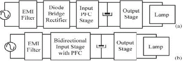
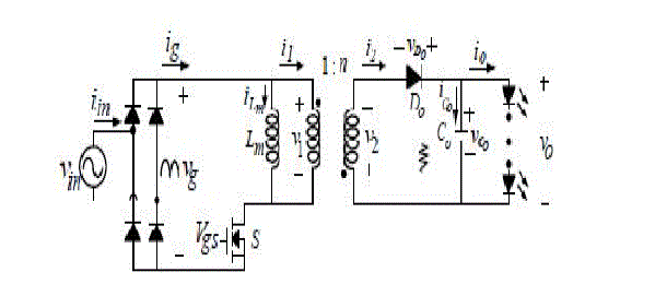
| The conventional system consist of an electromagnetic interference (EMI) filter plus a diode bridge rectifying stage in series with an input active power factor correction (PFC) stage. The output of this PFC stage supplies a capacitor, which provides the dc input voltage waveform for the output stage. For high-intensity discharge (HID) lamps supply, this output stage must address the current control, the current inversion, and the ignition.The novel topology proposed for the single-switch LED driver is based on a slight modification of the flyback converter. It is known that the flyback converter whenever operated in discontinuous conduction mode (DCM) provides inherent power factor regulation, because the input current follows the input voltage waveform, thus emulating a resistance for the power grid and providing close to unitary power factor. The derivation of the dimmable LED driver topology is done by taking a flyback single-stage PFC and sharing its power switch for dimming function, resulting in the topology presented in figure 1, where the switch M is also able to break the current applied to the LED array. |
| DISADVANTAGES OF THIS SYSTEM. |
| 1. The output voltage that converted from ccm boost converter is low. |
| 2. Power factor varies from 0.8 to 0.9. |
| 3. Temperature is HIGH. |
| 4. Lower reliability & durability as compared to proposed system. |
| 5. Efficiency is low as compared. |
| 6. Cost of the converter is high due to the presence of Diode Bridge Rectifier. |
PROPOSED DRIVER CIRCUIT
|
| This proposed system with the use of a flyback-based converter, which aims to remove the input diode bridge by using the integration of two power converter, each one for a different polarity of the input voltage. This System covers the comparison of both input topologies in terms of component count and in terms of efficiency, when used as PFC stages. However, as it will be commented later, the proposed topology has an extra feature as it can be also used in order to transfer energy to the power line. |
| A. Proposed system technique. |
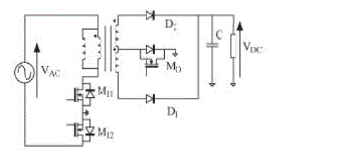
| At the input side the two flyback converter is connected in the reverse polarity; which reduce the input diode bridge. With the standard diode bridge + flyback PFC stage circuit, the proposed circuit provides about higher efficiency. Although the input diode bridge has been removed, the proposed circuit has two more MOSFETs and an additional diode, plus a secondary winding in the transformer. |
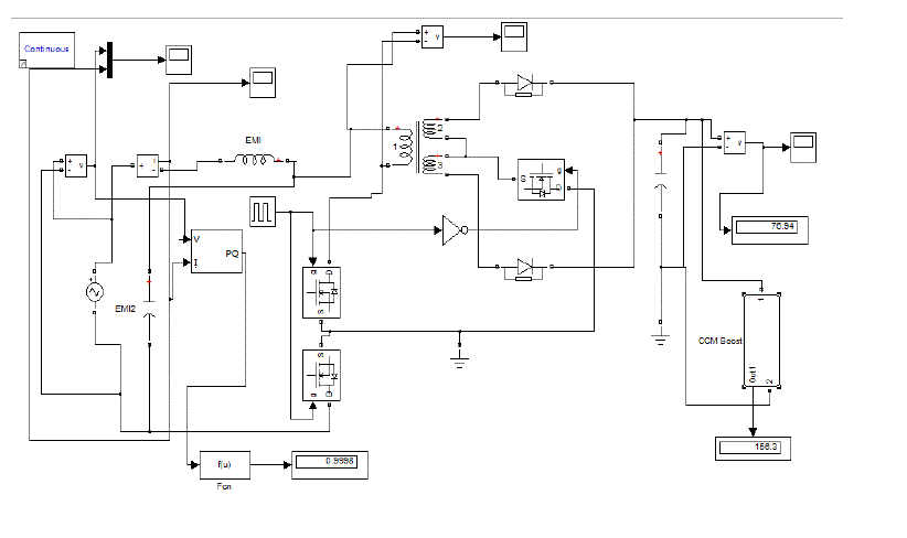
| fig.3. Proposed input stage based on the integration of two flyback stages with opposite polarities. This paper proposed is based on finding an optimized solution for the assembly formed by the diode bridge rectifier and the input PFC stage. The usual approach found in the literature makes use of a dc–dc converter after the diode bridge.The idea of this paper is to integrate two different flyback stages, one for each polarity of the line voltage, into a single two-polarity stage. This new approach is represented in above Fig.3.It must be noticed how this topology is directly supplied from ac mains, with no rectifying diode bridge. In the literature, several bridgeless input stages are used to avoid the losses of the input diode rectifier. |
| B. Circuit Operation. |
| The proposed driver circuit operation modes are done in three levels is explained in brief as follows |
| Operation under Positive Input Voltage |
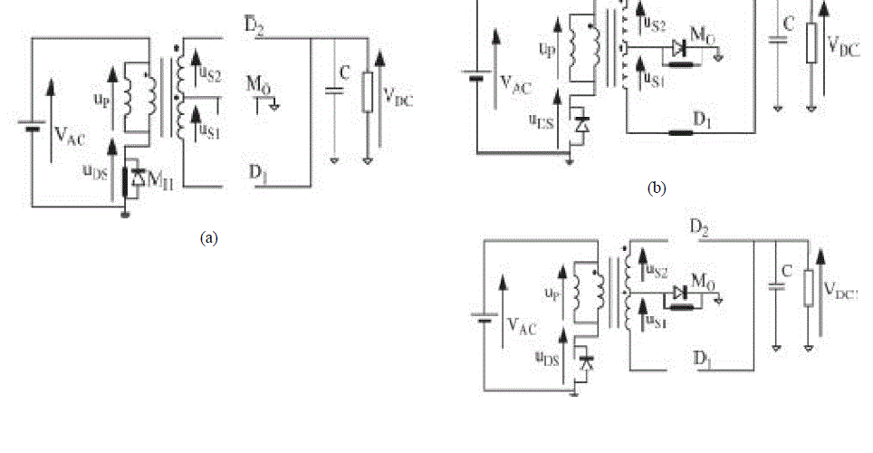
| For this paper, the discontinuous conduction mode (DCM) operation of the fly back stage will be considered. As shown in fig.4 (a). when switch MI1 turns on, the input line voltage, i.e., VAC, is applied to the primary side of the flyback transformer, i.e., up. The magnetizing inductance of the transformer begins to charge, whereas at both secondary sides, voltages uS1 and uS2 would be positive. The diode D1 is reversely biased, and thus, no current flows through the secondary winding connected to D1. On the other hand, D2 would be conducting with the polarity of the voltage uS2, and thus, the additional output MOSFET MO is necessary in order to block that current. Hence, MO must be turned off during this operation mode. Fig. 4 depicts the main voltage waveforms of the proposed circuit components, considering a positive input voltage.After this interval, MI1 turns off, and the magnetizing inductor discharges through the secondary side, forward biasing the diode D1. |
| Operation Under Negative Input Voltage |
| As shown in fig.4. (b). There is symmetry in the circuit with respect to the input voltage. In fact, the operation now is very similar to the one previously discussed, only interchanging the subscripts “1” and “2” in the previous discussion. The waveforms presented and the rest of considerations and conclusions are the same as in the previous analysis for ac line positive voltage. |
| considerations for the Output Stage |
| As shown in fig.4. (c). the proposed input stage delivers energy to a dc bus voltage. Depending on the final application, this dc voltage can present different characteristics. If HID lamp ballast is necessary, the dc capacitor does not present any special requirement, provided that it is able to withstand the voltage and current stresses that come from the design.The output stages should deal with the inversion of polarity of the lamp voltage waveform, with the low frequency stability of the arc discharge, with the ignition and warming-up processes, and with the avoidance of acoustic resonances. |
| C. Advantages of proposed electronic driver. |
| • Temperature is lower. |
| • Higher reliability & durability. |
| • Efficiency is improved. |
| • THD value is low. |
| • Bi directional converter. |
SIMULATION RESULTS
|
| The simulink design for the circuit 3. is designed and analised in the circuit 5. |
| Simulation Design Open Loop AC to DC. |
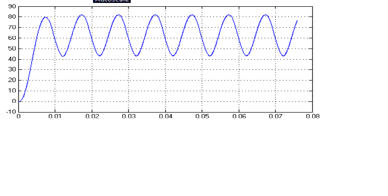
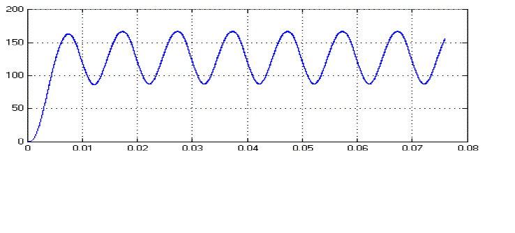
| A simulation designopen loop system as shown in Fig.5 is implemented in MATLAB SIMULINK with the help of coupled inductor, switches and diodes we get desired output voltage level(80V DC) (Fig.5), this 80V is boosted in to 153V (DC) from the CCM boost converter . |
| Simulation Design for closed loop with constant DC as input. |
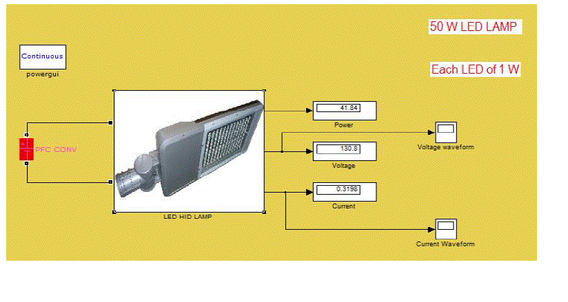
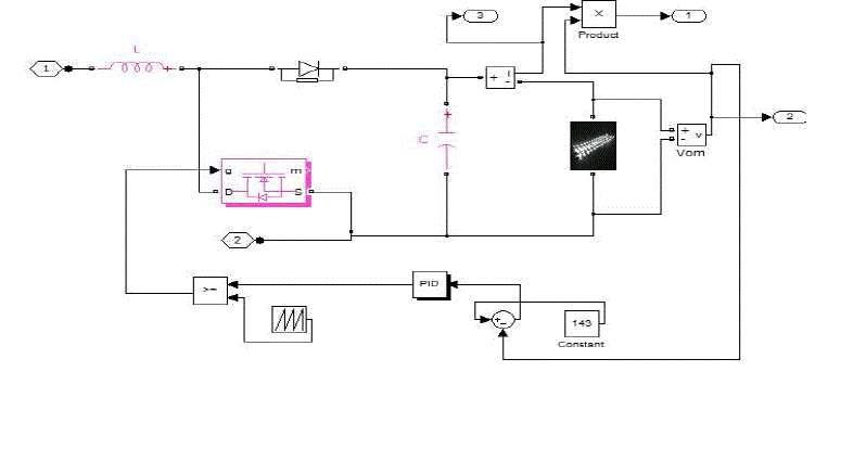
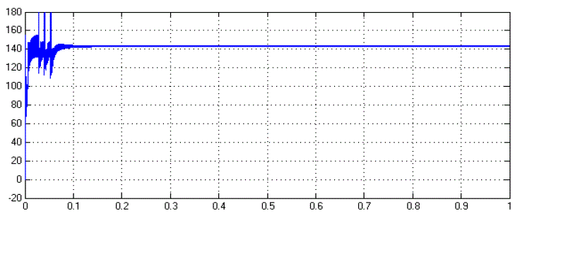
| A simulation designopen loop system as shown in Fig.8. is implemented in MATLAB SIMULINK with the help of coupled inductor, switches and diodes we get desired output voltage level (Fig.7). In this circuit we replace source as a constant dc source to increase to output and to get the effective results without distortions. |
CONCLUSION
|
| The results show better voltage and power factor than the conventional flyback-based scheme. Compared with the standard diode bridge + flyback PFC stage circuit, the proposed topology provides about better pf and voltage. Although the input diode bridge has been removed, the proposed circuit has two more MOSFETs and an additional diode, plus a secondary winding in the transformer. Thus, the temperature at these devices is lower than in the conventional circuit, which implies higher reliability and durability of the converter. In addition, it has been shown how the control pulses required for the proposed converter are easy to obtain from the conventional control scheme. The ability of the topology to operate as a bidirectional input, with a small variation in the proposed topology. However, the avoidance of the input diode bridge comes from the necessity of an input bidirectional stage. |
Figures at a glance
|
 |
 |
 |
 |
 |
| Figure 1 |
Figure 2 |
Figure 3 |
Figure 4 |
Figure 5 |
| |
 |
 |
 |
 |
 |
| Figure 6 |
Figure 7 |
Figure 8 |
Figure 9 |
Figure 10 |
|
| |
References
|
- M. Fellows, “A study of the high intensity discharge lamp-electronic ballast interface,” in Conf. Rec. 38th Annu. IEEE IAS Meeting, 2003, pp.1043–1048.
- W. Yan, S. Y. R. Hui, and H. Chung, “Energy saving of large-scale high intensity- discharge lamp lighting networks using a central reactive power control system,” IEEE Trans. Ind. Electron., vol. 56, no. 8, pp. 3069–3078, Aug. 2009.
- R. Orletti, M. A. Co, D. S. L. Simonetti, and J. L. de Freitas Vieira, “HID lamp electronic ballast with reduced component number,” IEEE Trans. Ind. Electron., vol. 56, no. 3, pp. 718–725, Mar. 2009.
- Y. Jang and M. M. Jovanovich, “Bridgeless high-power-factor buck converter,” IEEE Trans. Power Electron., vol. 26, no. 2, pp. 602–611, Feb.2011.
- N. Narendran and Y. Gu, “Life of LED-based white light sources,” IEEE J. Display Technol., vol. 1, no. 1, pp. 167–171, Sep. 2005.
- J. Garcia, A. J. Calleja, E. L. Corominas, D. Gacio, and J. Ribas, “Electronic driver without electrolytic capacitor for dimming high brightness LEDs,” in Proc. 35th Annu. IEEE IECON, Porto, Portugal, Nov. 2–5, 2009, pp. 3518–3523.
|