Keywords
|
| Double Drift structure, Transit Time diode, thermal runaway, Poisson equation, continuity equations , current density equations, heat equation, Terahertz regime, COMSOL Multi-Physics software. |
INTRODUCTION
|
| Terahertz technology is rapidly developing all over the world for its immense application possibilities in defense as well as civil sectors. In recent years the field of Terahertz technology has entered a completely new unprecedented expansion that is generating every growing level of broad based international attention (100 GHz-10000GHz). This extremely expansive and spectrally unique portion of the EM spectrum has applications in space based communication, upper atmospheric sensing, short range terrestrial communication and package screening. Systems for rapidly emerging applications at Terahertz frequencies require reliable high power sources. In the last few years the development of suitable sources for this frequency regime is being extensively explored worldwide. There is broadly two technology road map for Terahertz semiconductor devices. Approaching from the lower frequency range in the Terahertz regime, electronic devices such as Gunn diode, RTD FET have been widely investigated for Terahertz generation. From higher portion of Terahertz frequency spectrum, the photonics based devices, quantum cascade Laser (QCL) extends the emission wavelength to Terahertz spectral range. Most of the available Terahertz sources are complex and bulky in nature and not useful for operation at room temperature. |
| Avalanche Transit Time (ATT) Diodes which include IMPATTs, TRAPATTs, and BARITTs and so on are potential solid-state sources for Microwave power. In the past decade the advances in IMPATT device technology has made it possible to use this device in various communication systems operating in millimeter wave and sub-millimeter wave bands of frequency ranges which provides advantages such as increased resolution and use of low voltage power supplies. The availability of several atmospheric window frequencies in the mm-wave frequency range (30-300 GHz) has further increased the usefulness of IMPATT diodes which can now produce appreciable amounts of millimeter wave power at very high frequencies of operation at room temperature. Most of the available sub millimeter region IMPATT oscillators are fabricated from conventional Si. Conventional Si and GaAs based IMPATT diodes were found to be reliable but they are limited by power and operating frequencies due to the limitation imposed by their inherent material parameters. Wide Band Gap (WBG) semiconductor such as Silicon Carbide (SiC) has received remarkable attention during the last decade as a promising device material for high-temperature, high-frequency and high- power device applications due to its high thermal conductivity, high saturation velocity of charge carriers and high critical field for breakdown. |
| SiC exist in a number of polytypes for example 3C-SiC, 6H-SiC, 4H-SiC [1]. SiC devices can be made to have much thinner drift layer and higher doping concentration i.e they have very high breakdown voltage (600V and up) and yet with very low resistance relative to silicon device [2]. Resistance of high-voltage device is predominantly determined by the width of the drift region. In theory, SiC can reduce the resistance per unit area of the drift layer to 1/300 compared to Si at the same breakdown voltage. The larger bandgap also means SiC devices can operate at higher temperatures [3]. The guaranteed operating temperature of current SiC devices is from 150oC – 175oC. This is due mainly to thermal reliability of packages. When properly packaged, they can operate at 200oC and higher. |
| The huge material properties of SiC thus led the authors to choose SiC for designing a potential high power solid state IMPATT Oscillator at submillimeter wave region (220GHz) [3]. In the electromagnetic spectrum 220 GHz denotes a window frequency where atmospheric attenuation is minimum. In this paper the authors have designed and simulated a 220 GHz double drift SiC IMPATT diode and after that the 2D thermal modelling of the device has been done. |
THERMAL MODELLING OF 3C-SiC BASED IMPATT DDR
|
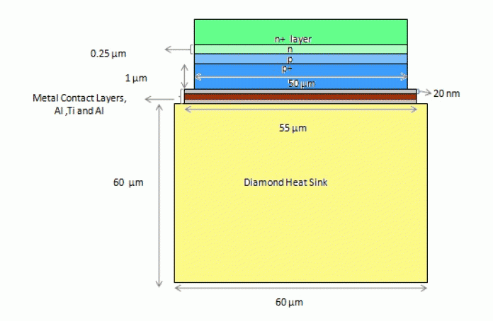
| The authors have used COMSOL MULTIPHYSICS software (version 4.3) for developing a model of a DDR Pulsed mode SiC based IMPATT diode to explain the heat transfer mechanism in the device. Here the author had followed the heat transfer by conduction method since the present model is for a solid-state high frequency device. This software uses some fundamental governing equations to simulate. These are Poisson equation, continuity equations , current density equations and the heat equation. In this paper, a 2D thermal model of Double Drift type diode as shown in Figure1 has been developed. In this structure, the authors have simulated an integrated heat sink type metalized (three layers of metallization with Al ,Ti & Al) DDR (Double drift region) n+ -n-p-p+ type simple structure. The structurelayers along with their dimensions based on transit time modeling approach as followed earlier [4][5], are shown in Figure 1.While modeling the device through this software, different materials are added to their corresponding geometric domains. SiC is the base- material and is added to the DDR structure.Type-II diamond is added to the heat sink and Aluminum and Titanium to the metallization layers. After that the simulated boundary heat source (8e10 W/m2) to the junction is introduced in the form of a rectangular current pulse of width 3μSec with ON time 100 ns. During the On time the junction temperature of the device increases and that is estimated using this software. During Off time the heat is dissipated from the device. At the end of the pulse the junction temperature of the device comes at ambient, and the second pulse train can be started to pass through the device.Finally the outflow of the heat at the junction is observed. |
RESULTS AND DISCUSSION
|
| Different thermal models for 3C-SiC based IMPATT DDR has been studied by using this software and the typical results obtained from this at different on times and off time are shown in the following figures. |
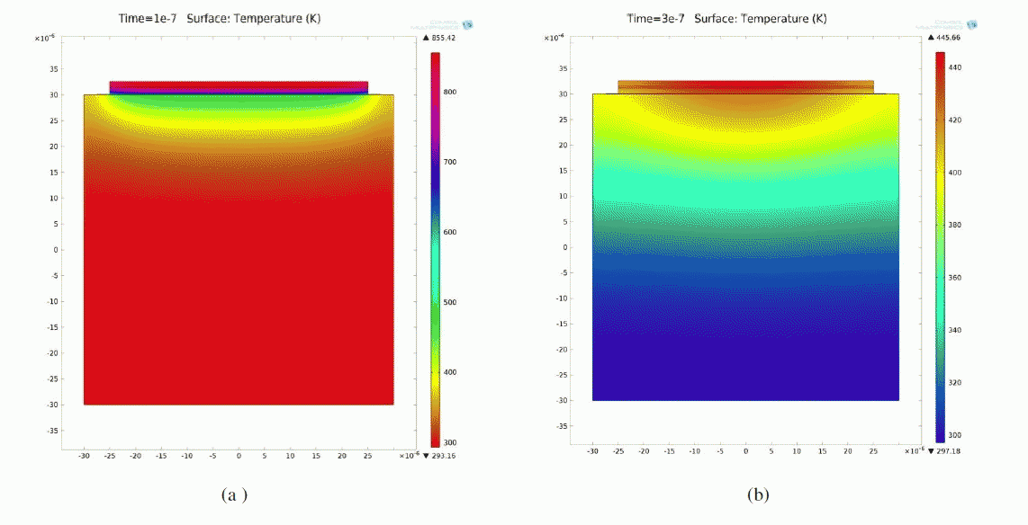
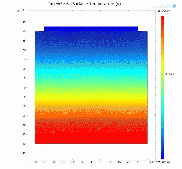
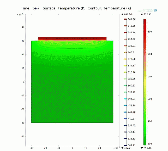
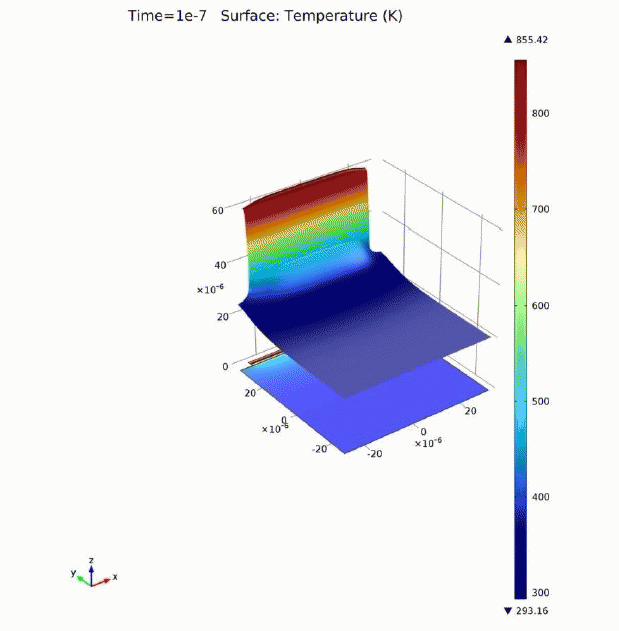
| The two dimensional heat distribution in 3C-SiC IMPATT DDR at ON times 100ns and 300ns are shown in figure2. Figure 3 denotes the heat distribution of same device during OFF time that is at 3μs. It is good to observe that during OFF time the junction temperature comes down to ambient temperature. The corresponding contour graph is shown in Figure 4. A 3D graph of heat distribution for the same at on time 100 ns is depicted in figure 5. |
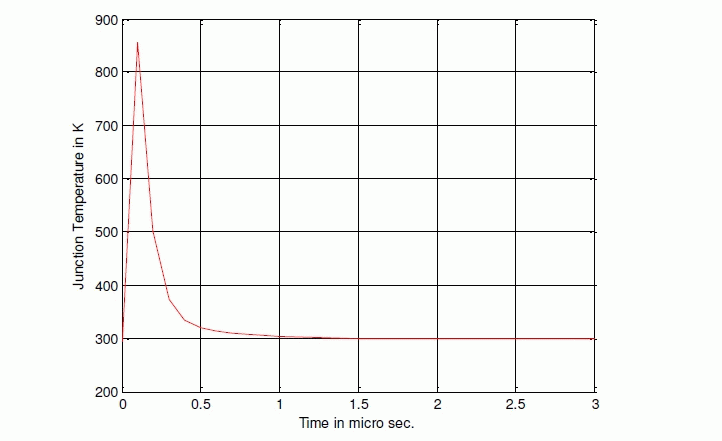
| A complete detailed set of results for temperature variation with time for the model is given in table 1. The corresponding temperature vs. time graph is plotted using MATLAB and is shown in figure 6. It can be analysed from the graphs that the temperature reaches its peak near about 100 ns and then gradually falls and attains the ambient temperature. |
CONCLUSION
|
| To the best of author’s knowledge, this is the first ever comprehensive studies on thermal modelling of SiC high power transit time device. The study will have immense application in military as well as civilian sectors, not only that, these devices are also suitable for application in biomedical sectors for early detection of malignant tumours etc. So in future this paper will act as a guide for researchers in device engineering. |
ACKNOWLEDGEMENT
|
| M.Mukherjee is thankful to Director, CMSDS for his kind permission to publish the work. P.De is grateful to Principal, SDET-Brainware Group of Institutions for his keen interest in this work. |
Tables at a glance
|
 |
| Table 1 |
|
| |
Figures at a glance
|
 |
 |
 |
| Figure 1 |
Figure 2 |
Figure 3 |
 |
 |
 |
| Figure 4 |
Figure 5 |
Figure 6 |
|
| |
References
|
- Moumita Mukherjee,“Silicon Carbide – Materials, Processing and Applications in Electronic Devices”, Ch.14, pp 337-368.
- Moumita Mukherjee, “ Physics and Technology of Silicon Carbide Devices”, Ch.14, pp 337-348.
- Moumita Mukherjee, “Advanced Microwave AndMillimeter Wave Technologies: Semiconductor devices, Circuits and Systems”, Ch.7, pp113-150.
- AritraAcharyya, Jayanta Mukherjee, Moumita Mukherjee and J. P. Banerjee, “Heat Sink Design for IMPATT Diode Sources with Different Base Materials Operating at 94 GHz”, Archives of Physics Research, vol.2, pp 107-126, 2011.
- AritraAcharyya and J. P. Banerjee, “Heat Sink Temperature Profile of Ring Geometry DDR IMPATT Diode”, Journal of Telecommunications, vol 6, pp 27-31,2010.
- Moumita Mukherjee et al, “Prospects of 4H-SiC Double Drift Region IMPATT Device as a Photo Sensitive High-Power source at 0.7 Terahertz Frequency Regime”, Active and Passive Electronic Components, 2008.
|