Keywords
|
| system-on-chip; low power; energy efficiency; high-performance; full duplex bus. |
INTRODUCTION
|
| Nowadays, there is a need of reduced interfaced complexity, low-cost and low-energy on-chip bus due to rapid growth of Internet of Things (IoT) market. Traditional bus protocols like the advanced microcontroller bus architecture (AMBA) advanced high-performance bus (AHB) [9] and advanced eXtensible interface (AXI) [3] from ARM Holdings, Wishbone from Silicore Corporation [4], Open Core Protocol (OCP) from OCP International Partnership [5] and CoreConnect from IBM [10] are commonly used in industry. The main characteristic of all these buses is that they transfer data linearly. However, There are some specific applications such as image processing, computer vision and wireless communication where data processing is usually based on the relationship of data neighbours, adjacency, connectivity, regions and boundaries [6],[8], and block data load and store [7]. In these cases, data transfer by block or matrix is preferable rather than by linear burst. In addition, for some advanced bus structures such as multi-bus and multilayer architectures, the bandwidth can be improved when maximum transactions occur in the same bus level or the same bus layer. However, these buses use a large number of wires for several set of bus signals and define complex hardware structures that are costly in terms of silicon area and energy consumption. These traditional bus-based architectures are also not suitableto the battery-driven portable devices due to features of high bandwidth and high energy consumption. |
| In order to overcome the above specified limitations of traditional buses, a low-cost and low-energy bus termed masterslave bus is introduced in brief. It is a dual bus structure as it is made up of control bus (MBUS) and data bus (SBUS). This protocol balances performance with cost, overcomes and implements features such as low power and high throughput. |
| The rest of the paper is organized as follows; the Section II givesbrief survey of all system-on-chip protocols. Section III gives their description in detail with necessary diagrams. Section IV illustrates the comparison between different onchip bus protocols. Section Vconcludes in brief. |
| ARM has developed AMBA [9] and AMBA AXI protocol [3] which are commonly used in various industries. Many protocols have been invented by different companies such as Wishbone Bus [4] from Silicore Corporation and Opencores; Open Core Protocol [5] from OCP Int. Partnership and CoreConnect [10] from IBM. Each protocol has its own significance and applied according to the need of system application. Many researches are working on protocols in order to optimize the protocol in terms of power consumption and hardware connection. |
DIFFERENT SYSTEM-ON-CHIP BUS PROTOCOLS
|
| The following are the bus protocols that are commonly used in industry. They are listed in as follows and are explained in brief as under. |
| 1. AMBA |
| 2. AMBA AXI |
| 3. WISHBONE BUS |
| 4. OPEN CORE PROTOCOL |
| 5. CORECONNECT BUS |
| 6. MSBUS PROTOCOL |
1) AMBA
|
| The Advanced Microcontroller Bus Architecture (AMBA) specification by ARM defines an on-chip communications standard which is required for designing high-performance embedded microcontrollers. AMBA comprises of three buses which are the Advanced High-performance Bus (AHB), the Advanced System Bus (ASB) and the Advanced Peripheral Bus (APB).Fig.1 shows a typical AMBA based architecture. It consists of a backbone bus which has the capability to sustain the external memory bandwidth where the on-chip memory, CPU and other Direct Memory Access(DMA) devices reside. |
| The AHB is mainly used for high-performance, high clock frequency system modules. It acts as the high-performance system backbone bus. It supports multiple bus masters, provides high-bandwidth operation and supports efficient connection of processors, off-chip external memory interfaces and on-chip memories with low-power peripheral macrocell functions. It implements features such as burst transfers, split transactions, single-cycle bus master handover, single-clock edge operation, non-tristate implementation and wider data bus configurations (64/128 bits). AHB Master, AHB Slave, AHB Arbiter, and AHB Decoder are the main components of the AHB. |
| The AMBA ASB specially defined for high-performance system modules is an alternative system bus which can be used whenever the high-performance features of AHB are not required. ASB implements most of the features of AHB which are required for high performance along with burst transfers, pipelined transfer operation and multiple bus master. ASB system design is composed of ASB Master, ASB Slave, ASB Arbiter, and ASB Decoder. |
| The AMBA APB acts as local secondary bus which is used for low-power peripherals and is enclosed as a single AHB or ASB slave device. AMBA APB is optimized for minimum power consumption and reduced interface complexity in order to support peripheral functions. The AMBA APB can be used to interface to any peripherals which are having low bandwidth and they do not require the high performance of a pipelined bus interface. In advanced version of APB, all signal transitions are only related to the rising edge of the clock. It enables the APB peripherals to integrate easily into any design flow with many advantages such as high-frequency operation, simplification of static timing analysis by the use of a single clock edge, etc. An AMBA APB comprises of a single APB bridge which is required to convert ASB or AHB transfers into a particular format for the slave devices on the APB and is responsible for bus handshaking and control signal retiming on behalf of the local peripheral bus. The function of bridge is to latch all address, data and control signals and to provide a second level of decoding to generate slave select signals for the APB peripherals. Another modules on the APB are APB slaves. [9] |
2) AMBA AXI
|
| The AMBA AXI protocol from ARM is intended at high-performance, high-frequency system designs and includes a number of features which are suitable for a high-speed submicron interconnects. The AXI protocol provides key features such as separate address/control and data phases, support for unaligned data transfers using byte strobes, burstarchitecture and design of the systems in which based transactions with start address only issued, separate read and write data channels to ensure low-cost Direct Memory Access (DMA), ability to issue multiple outstanding addresses, out-of-order transaction completion and easy addition of register stages to provide timing closure. |
| The generic architecture of AXI protocol is shown in Fig.2.It consists of AXI Master, Slave and Interconnect/Arbiter. The AXI Master is responsible for initiating transfers on bus whereas AXI slave responds to the request initiated by the master.AXI arbiter has the ability to take multiple masters at a time and arbitrates for the bus using configurable priority scheme. From Fig.2, this protocol provides a single interface definition for describing interfaces between a master and the interconnect; between a slave and the interconnect and between a master and a slave. |
| The AXI protocol is burst-based. In this protocol, every transaction has address and control information on the address channel that describes the type of the data to be transferred. The data is transferred between master and slave using a write data channel to the slave or a read data channel to the master. In write transactions, in which all the data flows from the master to the slave, the AXI protocol has an additional write response channel to allow the slave to signal to the master the completion of the write transaction. Fig.3 describes how a read transaction uses the read address and read data channels. |
| Fig.4 describes how a write transaction uses the write address, write data, and write response channels. The AXI protocol supports the variable-length bursts, from 1 to 16 data transfers per burst; bursts with a transfer size of 8-1024 bits; wrapping, incrementing, and fixed bursts; system-level caching and buffering control and secure and privileged access; atomic operations, using exclusive or locked accesses.[3] |
3) WISHBONE BUS
|
| One of the flexible design methodology for use with semiconductor IP cores is the WISHBONE System-on-Chip (SoC) Interconnection Architecture by Opencores and Silicore Corporation for Portable IP Cores. Its main purpose is to foster design reuse by overcoming System-on-Chip integration problems. This is achieved by creating a common interface between IP cores that improves the reliability and portability of the system, and results in faster time-to-market for the end user. Initially, IP cores used non-standard interconnection schemes that were difficult to integrate. By adopting a standard interconnection scheme, the cores can be integrated in quick and easy manner by the end user. WISHBONE interconnect is targeted as a general purpose interface which defines the standard data exchange between IP core modules.The WISHBONE interconnection makes system-on-chip and design reuse easy by creating a standard data exchange protocol. |
| The Wishbone consists of two interfaces, termed as master and slave. Master interfaces are IPs which are capable of initiating bus cycles, while slave interfaces are capable of accepting bus cycles. The hardware implementations have compatibility with various types of interconnection topologies such as crossbar switch interconnection (Fig.5), dataflow interconnection (Fig.6), Point-to–Point interconnection (Fig.7), and shared bus interconnection (Fig.8). |
| Crossbar switch interconnection mechanism allows modules to connect and communicate. Each connection channel can be operated in parallel to other connection channels, thus making the crossbar switches inherently faster than traditional bus schemes.The data flow interconnection is used when data is processed in a sequential manner. Here, each IP core has both a MASTER and a SLAVE interface.Data flows from one core to another core which is sometimes referred to as pipelining. They are used in linearsystolic array architectures for implementation of DSP algorithms. Point-to-point interconnection connects wishbone single master with a slave. The shared bus interconnection connects two or more MASTERs with one or more SLAVEs. In this case a MASTER initiates a bus cycle to a target SLAVE. The target SLAVE then participates in one or more bus cycles with the MASTER. |
| It includes features such as Simple, compact, logical IP core hardware interfaces that require very few logic gates; full set of popular data transfer bus protocols including READ/WRITE cycle, BLOCK transfer cycle and RMW cycle; Modular data bus widths and operand sizes; Supports both LITTLE ENDIAN and BIG ENDIAN data ordering;Supports single clock data transfers; Supports normal retry termination, cycle termination and termination due to error; User-defined tags which are useful for applying information to an address bus, a bus cycle or data bus; Master / Slave architecture for very flexible system designs; Multiprocessing capabilities which allows for a wide variety of System-on-Chip configurations; Arbitration methodology such as priority arbiter, round-robin arbiter, etc. is defined by the end user.[4] |
4) OPEN CORE PROTOCOL
|
| The Open Core Protocol (OCP) by OCP, International Partnership, defines a high-performance and a bus independent interface between IP cores which can be a simple peripheral core, a high-performance microprocessor, or it can be an on-chip communication subsystem such as a wrapped on-chip bus that reduces design risk, time, and manufacturing costs for SOC designs. The Open Core Protocol reuses the IP design by transforming IP cores, making them independent of they are used. It optimizes die area by configuring into the OCP interfaces and simplifies system verification and testing by providing a firm boundary around each IP core which can be observed, controlled, and validated. The OCP is similar to Virtual Socket Interface Alliance’s (VSIA) Virtual Component Interface (VCI).The Open Core Protocol hence, interface addresses communications between the functional units (or IP cores) which results in system on a chip. Figure 9describes SoC design based on the OCP protocol where a simple system contains a wrapped bus and three IP coreentities: one that is a system target, one that is a system initiator, and anentity that is both. |
| The Open Core Protocol provides features such as point-to-point synchronous interface; bus independence; commands such as read and write with five command extensions; 8-bit bytes (octets) address space; supports configurable data width to allow multiple bytes to be transferred simultaneously; supports pipelining of transfers; supports burst transfers; present tags in OCP interface controls the ordering of responses; supports the notion of multiple threads and supports sideband (or out-of-band) signalling.[5] |
5) CORECONNECT BUS
|
| The CoreConnect bus architecture was developed by IBM which simplifies the integration and reuse of processor, system, and peripheral cores within standard product and VLSI designs. Fig.10 shows CoreConnect Bus Architecture. |
| This architecture permits integrating custom SOC designs using cores designed according to the given specifications and lays the foundation of IBM Blue LogicCore Library or other non-IBM devices.The main elements of thisarchitecture comprises of the processor local bus (PLB) which is multi-master, synchronous and provides high bandwidth capabilities; the on-chip peripheral bus (OPB), a bus bridge, which is capable of executing fully synchronous operation, dynamic bus sizing, separate address and data buses and multiple OPB bus masters; and a device control register (DCR) bus which provides fully synchronous movement of GPR data between CPU and slave logic. The overall system performance is increased by connecting high-performance peripherals to the high-bandwidth, low-latency PLB and slower peripheral cores to the OPB, thereby reducing traffic on the PLB. Open architecture bus standard; presence of 32-, 64-, and 128-bit versions to support a wide variety of applications; enabling IP reuse in multiple designs and no-fee, no-royalty licensing are some advanced features of CoreConnect bus architecture. [10] |
6) MSBUS PROTOCOL
|
| MSBUS comprises of a master bus (MBUS) with a single master which can be microprocessor and slave bus (SBUS) with a single slave which can be a memory controller. The MBUS is a control bus which defines single transfer mode with at least one cycle command and one cycle data. As MBUS is defined with single master, it does not require any arbitration.It is responsible for low speed and low bandwidth functional register operations. It helps in reducing interface complexity and power consumption as number of wires for basic word size data bus is minimal when compared with other on-chip protocols.The timing diagram of MBUS protocol is shown in Fig. 11. A signal m_addr_wdata is created in MBUSas a shared bus with read address, write address, and write data information. A valid signal s_vld defined in MBUS is used to acknowledge the request that is required for synchronizing signals crossing between master and slave clock domain which avoids command FIFO overflows. A response delay timer is defined in the MBUS protocol in order to detect command errors. The command is indicated as “error” if the current response is a timeout and is retried or discarded by the master. |
| The SBUS is a data bus which is responsible for high-speed and high-bandwidth data transfers. Two handshake signals m_req and s_gnt are defined in SBUS which ensures that only one master occupies the read or write channel at a time. SBUS signals are classified into five packets: command which consists of transfer direction, size, and initial addressinformation; write packet; write data mask packet indicates the valid byte of the current word unit write data; read datapacket; and the respond packet which indicates that the current write data is ready or the read data is valid. The timingdiagram of SBUS protocol is shown in Fig.12. |
| The main feature of SBUS is that it supports block data transfer which is indicated by the most significant bit of data size signal,.len[10:0] for instance. If len[10] is considered as logic 1, the current transfer is a block transfer, len[9:6] denoting the width of the block and len[5:0] denoting the height of the block. Otherwise, it is defined as a linear transfer and all the other 10-bit signals denote the total transfer size.The block transfer mode ensures every memory boundary crossing commands predictable and computable by hardware. Hence, the time consumption of software configuration and bus commands is reduced. |
| Fig.13 shows typical MSBUS SoC Architecture. MSBUS is a dual-bus structure. The control bus is named as Master- Bus, because there is only one master themicroprocessor located on MBUS, likewise, the data bus isnamed as Slave- Bus, because there is only one slave located on SBUS via the DMA Controller. As shown in Fig. 13, all the peripherals such as UART, Timer,Serial Flash and GPIO, I2C devices are MBUS slaves. They are configured by softwarethrough MBUS directly. On the other side, all the devices such as USB,Bluetooth,Wifi arethe masters of SBUS and access the only slave memorythrough SBUS. |
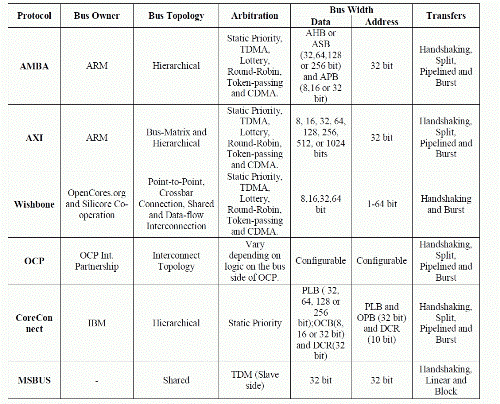
| The following table shows comparison of SoC buses w.r.t features such as topology,arbitration,bus width,etc. |
 |
CONCLUSION
|
| In this brief, we have done the survey of different on-chip protocols along with their features and architectures. A descriptive comparison between various on-chip protocols is made. MSBUS is efficient protocol as it can efficiently transfers block of data thereby reducing the hardware resources and minimal power consumption. This can be verified by implementing the MSBUS based DMA at RTL in HDL and comparing the same with other protocols by considering various parameters such as transfer time consumption, wire efficiency, valid data bandwidth, dynamic energy efficiency and power consumption. This is achieved by setting up Universal Verification Methodology (UVM) of given MSBUS SoC Architecture by integrating various ready-to-use configurable agents such as I2C, GPIO, USB, Bluetooth controller into test-bench and by application of various test cases. |
Figures at a glance
|
 |
 |
 |
 |
 |
| Figure 1 |
Figure 2 |
Figure 3 |
Figure 4 |
Figure 5 |
 |
 |
 |
 |
 |
| Figure 6 |
Figure 7 |
Figure 8 |
Figure 9 |
Figure 10 |
 |
 |
 |
| Figure 11 |
Figure 12 |
Figure 13 |
|
| |
References
|
- Xiaokun Yang and Jean H. Andrian, “A High-Performance On-Chip Bus (MSBUS) Design and Verification,” IEEE Transactions on Very Large Scale Integration (VLSI) Systems, Vol. PP, Issue: 99, July 2014.
- Xiaokun Yang and Jean H. Andrian,“A Low-Cost and High-Performance Embedded System Architecture and an Evaluation Methodology,”IEEE Computer Society Annual Symposium on VLSI(ISVLSI),July 2014.
- AMBA AXI Protocol v 1.0 Specification, ARM, 2003.
- Wishbone SOC Architecture Specification, Revision B.3, Silicore Corp., USA, 2002.
- Open Core Protocol Specification, OCP Int. Partnership, Beaverton, OR,USA, 2001.
- R. C. Gonzalez and R. E. Woods, Digital Image Processing, 3rd ed.Englewood Cliffs, NJ, USA: Prentice-Hall, Jun. 2012, pp. 68–99.
- MPEG-2 Standards Part 1 Systems,ISO/IEC,GE,Switzerland,Jun.2010.
- Wireless LAN Medium Access Control (MAC) and Physical Layer (PHY)Specification, IEEE Standard 802.11-1999, 1999.
- AMBA Specification, Rev 2.0, ARM, 1999.
- CoreConnect Bus Architecture, IBM, Yorktown Heights, New York, NY,USA, 1999.
|