Keywords
|
| Two Stage Buck Boost Converter(TSBB), Power LED Lamps, Discontinous Conduction Mode(DCM), Continuous Conduction Mode(CCM), Galvanic Isolation. |
INTRODUCTION
|
| As generally acknowledged, due to the high efficiency of the light-emitting diodes (LEDs), the LED is getting more and more attractive in the world, particularly for industrial applications in the street light. However, the high efficiency LED system needs the high efficiency power supply to feed the LED. The tungsten lamps provide only 8-10 lm/W and very inefficient, they are then replaced by fluroscent lamps now with the efficiency of an LED is as high as 100lm/W [2] they are mostly preferred. The main drawback of these LEDs is they needs constant voltage as input and they need current limiter before the input of the LED. |
| In general lighting applications, high power factor can be achieved using either a passive circuit or an active circuit. The passive circuit consist of inductors and capacitors together with uncontrolled rectifier. This is a good solution to achieve high power factor and does not generate electromagnetic interferences (EMI). In active power factor correction circuit, switch mode power supplies are used to achieve high power factor, low THD, and good output voltage regulation. Active power factor correction circuit is divided in to two categories, the two stage and single stage approaches. |
| A review of literature shows that a variety of LED power supplies and driver solutions, which can accurately control the current of the LED while achieving a near-unity input power factor, have been proposed [8],[10]. This drive is currently implemented with power electronic stages based on switch mode power supplies (SMPS). However, an electrolytic capacitor is required in these applications. Unfortunately, the operating life of such capacitors is by far shorter than the life of the HB LEDs, and usually are the shortest of all the devices in the power supply. Thus, removing the electrolytic capacitor would imply a remarkable increase in the operating life and reliability of the system [3],[4]. |
| PFC converters can be classified into two types: two-stage and single-stage. Two-stage PFC converters consist of a PFC stage and a dc/dc stage. Single-stage PFC converters integrate the PFC stage and the dc/dc stage, leading to simple topology and low cost. They are suitable for low-power applications [7]. The simplest active PFC circuits are implemented with a single-stage that makes the power factor correction. The most common single-stage topology used is the flyback converter [5], [6] working in Discontinuous Conduction Mode (DCM), being called DCM flyback PFC converter. The main drawbacks of these pre-regulators are, by one hand, the high peak current stresses caused by the DCM and serious EMI problem [3] and, by the other, the poor dynamics that these converters perform due to the lowpass filter (10 Hz-20 Hz) needed to reduce the input line current total harmonic distortion (THD). Therefore, if dimming operation is required, which must be done at frequencies above 200 Hz, these single stage solutions are not feasible . Attending to the re asons exposed above, a two-stage is needed so the Power Factor Correction can be done properly and a fast enough output dynamics is obtained. |
| A two stage buck boost converter (TSBB) is proposed to supply power LED lamps from the ac mains, providing high power factor (PF), low LED current ripple, and high efficiency. With the double buck boost converter, two converters are cascaded with a single switch and it includes two low value inductors and capacitors and suitably placed diodes thus the LED lamp can be supplied with low ripple and high efficiency power. In Section II, the working of TSBB converter with isolation [1] is presented. In Section III, the analysis and design of the TSBB converter [1] in various mode is detailed. In Section IV, Simulation results of TSBB converter with isolation is discussed. Section V discusses on the laboratory prototype made and in the Section VI results and conclusions are discussed. |
TWO STAGE BUCK BOOST CONVERTER
|
| Fig 2 shows the schematic circuit of the TSBB converter. This converter acts as a two buck-boost converters which are electrically isolated and connected to the load. The input buck-boost converter is made up by L1, D2, D3, CB and M1 and the output buck-boost converter acts as a flyback converter due to addition of galvanic isolation and comprises of LO, D3, CO, M1. The reversing polarity produced by the first converter in the capacitor CB is corrected by the second converter, given a positive output voltage with respect to ground, thereby simplifying the measurement of the load current, in the closed-loop operation, also reducing the sensing circuitry and hence the cost. |
| The input inductor Li is operating in discontinuous conduction mode (DCM), the average current through the line will be almost in phase with the line voltage, which results in a line power factor near unity, this is important if the converter operates from mains voltage in a grid. Also, the output inductance LO can be operated either in continuous conduction mode (CCM) or discontinuous conduction mode. DCM results in a bus voltage across CB that is independent of duty cycle and output power. But there is a drawback in DCM, it requires a higher value of the output capacitance to achieve low current ripple through the load. So to avoid high current ripple in the output and to reduce the value of the output capacitance, CCM operation is preferred. Inaddition to above, to reduce the ripple voltage occurring at low frequencies, the second stage of the TSBB is operated with D = 50% (duty cycle), since the duty cycle is multiplied by the buckboost converter voltage ratio. In this way, it will be possible even to use a film capacitor to implement the output capacitance; this gives the TSBB converter longer life rating and improved efficiency over the use of electrolytic capacitors. |
| Moreover, with a careful design of the converter, the bus capacitor can also be made low enough to be implemented with film technology, thus avoiding the low life rating electrolytic capacitors in the whole converter. This implies the design of the converter so that it operates with a α lower than 0.5. In this manner, the output converter voltage ratio will be lower than one, thus reducing the low frequency voltage ripple in the same amount. |
(a) Need for Isolation
|
| Non isolated switching regulators are very commonly used regulators because of low cost and simple. These converters suffer from one disadvantage in that there is an electrical connection between the input and output. Many safety agency bodies require a separation from the applied input voltage and the output voltage which is often user accessible. An isolated DC-DC converter will have a high frequency transformer providing that barrier. This barrier can withstand anything from a few hundred volts to several thousand volts, as is required for medical application.In this particular LED application, these are widely used for high power lighting applications .therefore it is essential to isolate higher power load and low power control part. A flyback transformer is used here to provide the requirement. |
ANALYSIS OF TSBB CONVERTER
|
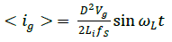
| `In this section, the TSBB converter with isolation is analysed when operated from the main voltage, achieving a near unity input PF and a low ripple current through the power LED load. The line voltage is assumed to be sinusoidal waveform given as vg(t)= Vg sin wLt. |
(a) Line Current
|
| The input current ig corresponds to the current through the inductance Li during the time interval 0-DTS, where D is the transistor duty cycle and TS is the transistor switching period. This current is modulated by the rectified line voltage [1]. Thus, the value of the input current averaged at line frequency can be calculated as follows [1]. |
 (1) (1) |
| Where, fs is the switching frequency, Vg is the peak line voltage and wL is the line angular frequency. From the above equation, the averaged input current is a sinusoidal waveform that will provide an input PF close to unity once filtered by the input electromagnetic interference (EMI) filter. The mean input power Pi can be calculated as, |
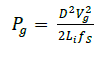 (2) (2) |
(b) Output and Bus Voltages
|
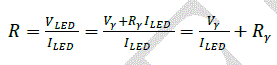
| The output voltage VO for the ideal converter can be obtained by equating input and output power is obtained as follows: |
 (3) (3) |
| Where, R being the static equivalent resistance of the LED load which can be obtained by the ratio between the dc values of LED voltage (VLED) and current (ILED) at each operating point. |
 (4) (4) |
| Where, Vγ and Rγ are the voltage and resistance parameters of the LED lamp. Assuming 100% efficiency, by equaling (2) and (3), the output voltage is obtained by, |
 (5) (5) |
| Where, K is a nondimensional factor given by, |
 (6) (6) |
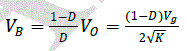
| Since the output stage corresponds to a buck boost converter operating in CCM, the bus voltage VB will be, |
 (7) (7) |
| As can be seen from (5) and (7), when operating the input stage in DCM and the output stage in CCM, the bus and output voltages are reversely dependent on the duty cycle. The sum of both voltages does not depend on the duty cycle, being only proportional to the line peak voltage, |
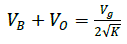 (8) (8) |
(c) Energy Transferring Components or Reactive Component
|
| The value of the energy transferring element at the input which is Li is calculated based on the output power and assuming 100% efficiency the value of inductance is so obtained to be, |
 (10) (10) |
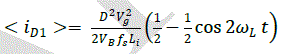
| The bus capacitor CB is calculated to limit the low frequency ripple of the bus voltage, which is the voltage applied to the second stage. The current through this capacitor is given by the currents through diodes D1 and D2. In these diodes, only the current through D1 is modulated by a rectified line frequency. In order to calculate the bus ripple, the low frequency component of the current through D1 must be obtained. The average current through D1 is, |
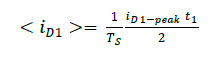 (11) (11) |
| Where,iD1-peak is the peak current through D1 in each switching period and t1 is the time needed by this current to reach zero. Both values changing after double the line frequency and have the following values. |
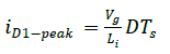 (12) (12) |
 (13) (13) |
| D1 average current is, |
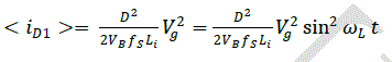 (14) (14) |
| Above equation becomes, |
 (15) (15) |
| Then, the low frequency ac component circulating through D1 and CB is given by, |
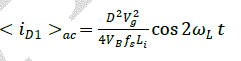 (16) (16) |
| The low frequency peak to peak ripple voltage across capacitor CB , ΔVBLF can be obtained as, |
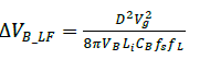 (17) (17) |
| The bus capacitance CB , for a given peak-to-peak ripple in the bus voltage is then calculated from (17) as follows: |
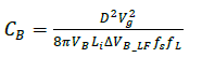 (18) (18) |
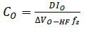
| Note that, as long as the output buck-boost converter operates in CCM, the LED current ripple at low frequency depends only on the bus voltage ripple and thus, on the bus capacitance CB. The output capacitance CO has no effect on this low frequency ripple. Finally, the output inductance and capacitance LO and CO are obtained using the well known expressions for a buck-boost converter operating in CCM, |
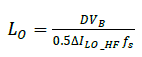 (19) (19) |
 (20) (20) |
| Where, ΔILo_HF is the LO high frequency peak-peak current ripple, ΔV0_HF is the high frequency peak-to-peak output voltage ripple, and Io is the dc current through the LED load. |
SIMULATION RESULT AND DISCUSSIONS
|
| Simulation of the TSBB converter with isolation was done using MATLAB Software. Simulation is done with the help of Simulink of Matlab 7.8.0 version. MATLAB is one of the most popular software in control field and its graphical simulation environment SIMULINK is very suitable for dynamic system simulation because there are plenty of toolboxes and modules. Simulink is a software package for modeling, simulating, and analyzing dynamic systems. Simulation results are very useful for deciding the ratings of the different components for hardware implementation. With the help of simulation results, the relevant waveforms are successfully obtained. |
| A simulation prototype for a street lighting application has been developed using MATLAB/SIMULINK. The lamp is formed by 60 LW W5SG power LEDs by Osram in a series array. The load rating current is 350 mA, with an output power of 70Wand a total luminous flux of 1500 lm. The load was tested at the laboratory, obtaining the following model parameters: Vγ = 170 V and Rγ = 87Ω. The equivalent load resistance at nominal power is R = 570 Ω. The selected switching frequency is 50 kHz. The line voltage is 230 Vrms with a 50-Hz line frequency. The converter must admit at least 10% line voltage variation, assuring constant current through the load. The switching frequency is assumed to be 50 KHz. The output voltage obtained to be 200 V. |
| The circuit configuration shown in fig 7, TSBB converter with isolation in closed loop mode using a PI controller. The values of the PI controller elements are so chosen to give a reduced steady state error. |
| The figure 8 represents the input voltage and current waveform of the proposed converter. From the graph we can see that the input voltage is inphase with averaged input current, so the power factor becomes unity and it also shows the output voltage with low ripple current of the proposed converter. |
| The figure 9 represents the current and voltage waveform through the inductor and switch and also shows the voltage and current waveforms across diode D3. |
| The figure 10 represents current and voltage waveforms across the diode D1and also shows the voltage and current across diode D2. |
CONCLUSIONS
|
| A two stage buck boost converter (TSBB) with isolation has been successfully simulated in this paper. This circuit configuration is suitable for low power applications. In closed loop mode suitable controller namely the PI controller was used. From the above section, it is evident from the results that the configuration of TSBB with isolation in closed loop is efficient compared to the converters using more than one switch. |
| The added advantage of this converter is that this is suitable for power converters used for medical applications where isolation is essential. Though isolation may end up in increase of cost, it is a safety aspect that cannot be neglected in certain application. Thus TSBB converter with isolation in closed loop mode is more efficient, safe and reliable for any low power loads. |
Figures at a glance
|
 |
 |
 |
 |
 |
| Figure 1 |
Figure 2 |
Figure 3 |
Figure 4 |
Figure 5 |
 |
 |
 |
 |
 |
| Figure 6 |
Figure 7 |
Figure 8 |
Figure 9 |
Figure 10 |
|
| |
References
|
- J.Marcos Alonso, Juan Vina, David Gacio Vaquero, “Analysis and Design of the Integrated Double Buck Boost Converter as a High powerfactor driver for power LED Lamps”, IEEE Transactions on industrial electronics, vol.59, no.4, April 2012.
- D. Gacio, J. M. Alonso, J. Garcia, L. Campa, M. Crespo, and M. Rico- Secades, “High frequency PWM dimming technique for high powerfactor converters in LED lighting”, in Proc. 25th Annu. IEEE APEC, Feb. 21–25, 2010, pp. 743–749.
- J. Garcia, A. J. Calleja, E. L. Corominas, D. Gacio, and J. Ribas, “Electronic driver without electrolytic capacitor for dimming high brightnessLEDs”, in Proc. 35th Annu. IEEE IECON, Nov. 3 –5, 2009, pp. 3518–3523.
- Y.X.Qin, H.S.H. Chung, D.Y.Lin, S.Y.R.hui, “Current Source Ballast for high Power Lighting Emitting Diodes without ElectrolyticCapacitor”, IEEE IECON 2008, 34th Industrial electronics Annual Conference, Proceedings of, pp. 1968- 1973, 10-13 Nov. 2008, Orlando,Florida, USA.
- Chien Ming Wang, “A novel single stage high power factor electronic ballast with symmetrical half bridge topology”, in IEEE Transactions.Industrial electronics. vol.55 no-2 pp 969-972, feb 2008.
- Tsorng-juuliang, Chien-minghuang, and Jiann-fuhchen, “Two stage high power factor electronic ballast for metal halide lamps”, in IEEETransactions on Power electronics, vol.24, no.12 december 2009.
- John C, W. Lam and Praveen k jain “A high-power-factor single-stage single-switch electronic ballast for compact fluorescent lamps”, in IEEETransactions on Power electronics, vol.25, no.8, august 2010.
- H. Broeck, G. Sauerl¨ander, and M. Wendt, “Power driver topologies and control schemes for LEDs”, in Proc. IEEE APEC 2007, pp. 1319–1325.
- J. Sebasti´an, D. G. Lamar,M. Arias, M. Rodr´Ãâñguez, andM.M. Hernando, “A very simple control strategy for power factor correctors drivinghigh brightness light-emitting diodes,âÃâ¬Ãâ in Proc. IEEE APEC 2008, pp. 537–543.
- S. Y. (ron) hui, Sinanli, Xuehuitao,Wuchen, and W.M.ng , “A novel passive offline led driver with long lifetime”, in IEEE Transactions onPower electronics, vol.25, no.10, October 2010.
- XiaogaoXie, Jian Wang, Chen Zhao, Qiang Lu, and Shirong Liu, “A Novel Output Current Estimation and Regulation Circuit for PrimarySide Controlled High Power Factor Single-Stage Flyback LED Driver”, IEEE Transactions on Power Electronics, vol.27, no.11, November2012
- K. I. Hwu, Y.T.Yau,, and Li-Ling Lee, “Powering LED Using High efficiency SR Flyback Converter”, in IEEE Transactions on IndustrialElectrons vol.47, no.1, Jan/Feb 2011.
- Hongbo ma, Jih-sheng lai, Quanyuanfeng, Wensongyu, Cong zheng, and Zhengzhao, “A novel valley-fill sepic-derived power supply without electrolytic capacitors for led lighting application”, in IEEE Transactions on Power electronics, vol.27, no.6, june 2012.
|