Keywords
|
| Bridgeless Rectifier, SEPIC converter, Discontinuous Conduction mode (DCM), Power Factor Correction(PFC),Zero Current Switching(ZCS) |
INTRODUCTION
|
| The preferable type of power factor correction (PFC) circuit is the active PFC since it makes the load behave like a pure resistor, leading to near unity load power factor and generating negligible harmonics in the input line current. Most active PFC circuits as well as switched mode power supplies (SMPS) on the market today comprise a front-end bridge rectifier followed by a high frequency dc-dc converter. Several of the most popular topologies for PFC converters are the followings: fly-back converter, buck-boost converter, boosts converter, SEPIC converter and CUK converter. The boost PFC converter and the SEPIC PFC converter are briefly introduced to compare their advantages and disadvantages. |
| In addition, the bridgeless SEPIC topology is introduced to discuss its advantages over converter switch rectifying diodes. The boost converter is the most popular PFC device because of its simple power circuitry and simple control scheme arising from its single-switch and ground-referenced switch design [2]. Furthermore, low input current distortion could be the reason why the boost converter is so popular for PFC applications. However, the boost converter is limited by the fact that its input voltage must be smaller than its output voltage. This disadvantage requires an additional dc/dc stage for LED applications. Single-ended primary-inductor converter (SEPIC) is a type of DC-DC converter allowing the electrical potential (voltage) at its output to be greater than, less than, or equal to that at its input. The output of the SEPIC is controlled by the duty cycle of the control transistor. A SEPIC is similar to a traditional buck-boost converter, but has advantages of having non-inverted output. The advantage of the SEPIC converter is that its output voltage is not necessarily limited by its input voltage range. This property means that the output voltage can be higher or lower than input voltage. Moreover, this property means that the SEPIC PFC converter does not require an additional dc/dc stage for applications [5]. Additionally, the SEPIC converter can reduce the input current ripple by incorporating 2 properly wound inductors. This characteristic means that the power loss due to the current ripple can be reduced. The absence of an input diode bridge and the presence of only two semiconductor switches in the current flowing path during each switching cycle results in less conduction losses.Bridgeless PFC topologies are currently gaining increasing interests. Generally, bridgeless PFC converters suffer from the difficulty of implementation and control, but bridgeless topology can reduce conduction losses from rectifying bridges; thus, overall system efficiency can be increased. In addition, a bridgeless topology has the advantage of total harmonic distortion (THD) decreasing from input diode reduction. |
| The bridgeless SEPIC PFC converter circuit is typically popular for bridgeless topologies, in which the converter operates separately over positive and negative cycles [5]. This circuit is simple and easy to implement, there are fewer limitations to choosing the main passive components. This circuit can be modified into a single-switch bridgeless converter, which has low conduction loss and requires fewer components. Each topology has advantages and disadvantages regarding to the output voltage limitation, the difficulty of controller implementations. Furthermore, for electric vehicle applications, the input must be lower than the ac input voltage. Usually, this voltage ranges from 12V to 50V.Therefore, if a boost converter--the most famous and simplest topology—is adopted, then a second stage is needed to supply proper input power for electric vehicle applications [2].SEPIC with single stage can also be implemented. Considering the above-mentioned advantages and disadvantages, a SEPIC PFC converter can be a good choice if the controller is designed with accurate modelling single-switch bridgeless SEPIC PFC converter operating in discontinuous conduction mode (DCM) is used in Simulink diagram. |
| This paper is devoted to a new power circuit topology to be implemented bridgeless sepic for PFC, without any additional component above said problems are overcome. |
DISCRIPTION OF SEPIC CONVERTER
|
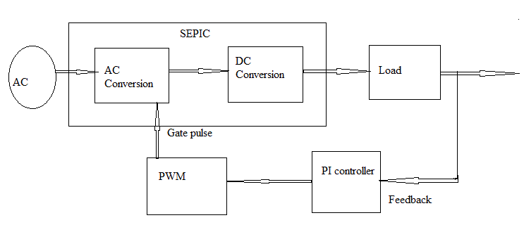
| SEPIC is a type of DC-DC converter allowing the electrical potential at its output to be greater than, less than, or equal to that to its input. The output of the SEPIC is controlled by the duty cycle of the power switches. A SEPIC is similar to a conventional buck-boost converter, except it has advantages of having non-inverted output(the output has the same voltage polarity as the input) capable of true shutdown: when the switch is turned off SEPIC are useful in applications in which battery voltage can be above and below that of the regulator's intended output Fig.2 shows the block diagram of proposed sepic rectifier AC input is given to the AC conversion side in which we using two same value inductors connected in parallel[8]. It will smooth the supply voltage and in the DC conversion side the diode will combine the voltage of two half cycle of supply voltage. The output from this block is given to the load through output capacitor. PI controller is used to form a closed loop to control the duty cycle of the switches in order to maintain the input current in phase with input voltage. |
| The absence of an input diode bridge and the presence of only two semiconductor switches in the current flowing path during each switching cycle results in less conduction losses. Unlike the boost converter, the Sepic converters offer several advantages in PFC applications ,such as easy implementation of transformer isolation, inherent inrush current limitation during start-up and overload conditions, lower input current ripple, and less electromagnetic interference (EMI). |
A.SEPIC Converter operating principle
|
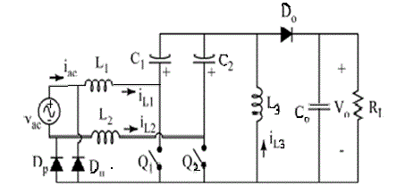
| The bridgeless rectifiers shown in Fig.2 are constructed by connecting two dc–dc converters. Referring to Fig. ,2 during the positive half-line cycle, the first dc–dc Sepic circuit L1,Q1,C1,L3,Do is active through diode Dp, which connects the input ac source to the output ground. During the negative half-line cycle, the second dc–dc Sepic circuit, L2,Q2,C2,L3,Do, is active through diode D, which connects the input ac source to the output ground. Thus, due to the symmetry of the circuit, it is sufficient to analyze the circuit during the positive half-period of the input voltage. These advantages include the following: there is natural near unity power factor, the power switches are turned on at zero current and the output diode Do is turned off at zero current [9] |
| Thus, the loss due to the turn-on Switching losses and the reverse recovery of the output diode are considerably reduced. In the output side PI controller is used to make the feed back to vary the duty cycle of the power switches. PI controller is used to form a closed loop to control the duty cycle of the switches in order to maintain the input current in phase with input voltage proposed sepic with PI will provide . Active wave shaping of the input current, Filters the high frequency switching, feedback sensing of the source current for waveform control, feedback control to regulate output voltage. The input ac line voltage is always connected to the output ground through the slowrecovery diodes Dp and DO [12]. Thus, the proposed topologies do not suffer from the high common-mode EMI noise emission problem and has common mode EMI performance similar to the conventional topologies. The two power switches can be driven by the same control signal, which significantly simplifies the control circuitry. When operating a converter in the DCM region, the current stress on the converter components becomes relatively large compared to the CCM operation, and this leads to one disadvantage of the DCM operation, which limits this operating mode to low-power applications (< 300 W)[4]. Voltages and currents are normalized with respect to the peak input voltage Vm and output load current (Vo/RL), respectively.A single stage AC-DC topology with power factor correction is proposed for battery charger applications. Desired features for battery charger such as low cost, fast charging, charge profile programmability, high efficiency and high reliability are fully achieved by means of proposed solution[13]. Additionally, its multiphase operation configuration provides easy power scaling. |
| The proposed approach is superior to conventional converter regulation widely used for EV (Electrical vehicle) charger applications. It is especially suitable to low cost and high power applications. The feasibility and practical value of the proposed approach are verified by the experimental results from a 1 kW product prototype. |
| Battery chargers for consumer and industry markets must be precise in function and reliable in operation at reasonable manufacturing cost. Battery chargers fall in to a group of electrical loads called “inductive” loads. Inductive electrical loads are characterized by two different power designations-watts(w) and volt-amps(VA).A battery charging system has a first rectifier adapted for converting an AC voltage at an input thereof to a first DC voltage at an output. |
| A power factor correction (PFC) circuit coupled to the first rectifier, for correcting the power factor of the battery charging system and outputting a second DC voltage [15]. a first power converter coupled to the PFC circuit, for converting the second DC voltage to a third DC voltage a second power converter coupled to the first power converter, for converting the third DC voltage to a fourth DC voltage to be delivered to a battery and a first controller adapted for sensing the fourth DC voltage at the output of the second power converter for regulating the second power converter to maintain the fourth DC voltage at a predetermined value [20]. |
TUNING OF PI CONTROLLER
|
| PI controller makes a closed loop to control the power factor during load regulation. PI is a control feedback mechanism widely used in industrial applications. It corrects the error between a measured variable. A desired set point by calculating and initiating a corrective action that can adjust the process accordingly and rapidly, to keep the error minimal. |
| General approach to tuning: |
| • Initially have no integral gain |
| • Increase KP until get satisfactory response |
| • Start to add in integral until the steady state error is removed in satisfactory time(may need to reduce KPif the combination becomes oscillatory) |
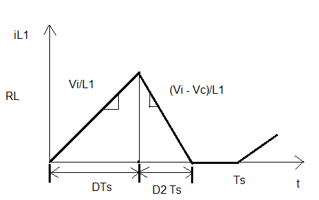
| DCM for the proposed rectifier occurs when the current through diode Do drops to zero before the end of the switch off-time. Thus, the circuit operation during one switching period Ts in a positive half-line period can be divided into three distinct operating modes. |
DCM OPERATION
|
| In which circuit voltages and currents are zero for a brief time interval. During this unique interval, a new and third circuit topology combination not normally allowed is now possible. |
| This is called the DCM mode and will turn out to be a big practical advantage in several ways. In the DCM mode the DTs interval is usually unchanged because the transistor conduction is controlled solely by the control signal, which is independent of circuit operation. However, the D’T period is divided by circuit conditions into two new portions often called D2, and D3. The diode conduction duration depends solely on the circuit conditions which change during the D’Ts interval to shut –off the diode prematurely. When turn-off occurs depends on the load conditions. |
| D2 or D3 in DCM operation becomes an additional unknown in addition to D. This division of the D’ intervalinto D2 and a new D3 interval usually happens when I(out) has a minimum DC value called the critical current, Icritical. DCM usually occurs at light load and Vout jumps up from its CCM value, sepic converter, to a higher value output-voltage. This can be very useful for power supplies employed for starting fluorescent lights, which initially have zero load. |
STAGES OF OPERATION
|
| When the switch Q1 is turned on, diode Dp is forward biased by the sum inductor currents iL1 and iL2. As a result, diode Dn is reversed biased by the input voltage. The output diode is reversed biased by the reverse voltage (vac + Vo). In this stage, the three inductor currents linearly increase at a rate proportional to the input voltage vac.The rate of increase of the three inductor currents. At the instant tl, switch Q1 is turned off, diode Do is turned on, simultaneously providing a path for the three inductor currents. Diode Dp remains conducting to provide a path for iL1 and iL2. In this stage, the three inductor currents linearly decrease at a rate proportional to the output voltage Vo. This interval ends when the output diode current I smoothly reaches to zero and Do becomes reverse biased. In this stage, both Q1 and Do are in their off-state. Diode Dp provides a path for i??3. The three inductors behave as current sources, which keeps the currents constant. Hence, the voltage across the three inductors is zero. Capacitor C1 is charging up by i??1, while C2 is discharged by i??2. |
| When operating a converter in the DCM region, the current stress on the converter components becomes relatively large compared to the CCM operation, and this leads to one disadvantage of the DCM operation, which limits this operating mode to low-power applications (<300 W). Voltages and currents are normalized with respect to the peak input voltage Vm and output load current (Vo/RL), respectively. |
SIMULATION RESULTS
|
| The modified bridgeless sepic converter operating in discontinuous conduction mode. It composed of two sepic each will be operating in each half cycle of the input supply voltage. The output to input relation is controlled by PI controller. The proportional controller checks the error between actual and reference voltage. The integral controller will compensate the error by comparing error with repeated sequence. The value again compared with PWM signal. Output from PI controller is compared with repeated sequence. This is the sequence to produce reference signal. Compared value given to the relay block to produce arbitrary output. The Boolean block will produce the binary output required for logical operation. This makes to produce pulses for switches by using logical NAND operation. The simulation result for power factor correction is shown below. |
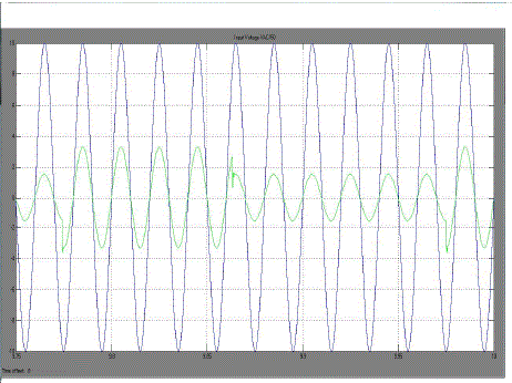
| Above Fig. 4 shows that power factor are during voltage is regulated at 100v. So, that at any time, the line current is in phase with the input line voltage. Line current in phase with line voltage will improve the Power factor of this circuit. This improved power factor will increase system reliability. |
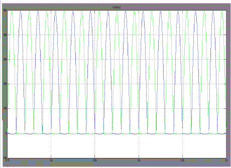
| Above fig 5 will shows the alternate switching of two switching of power switches second will shows the inductor current whenever the inductor current goes to zero the switch will be turned on. So the switching stress across the switch will be minimized. |
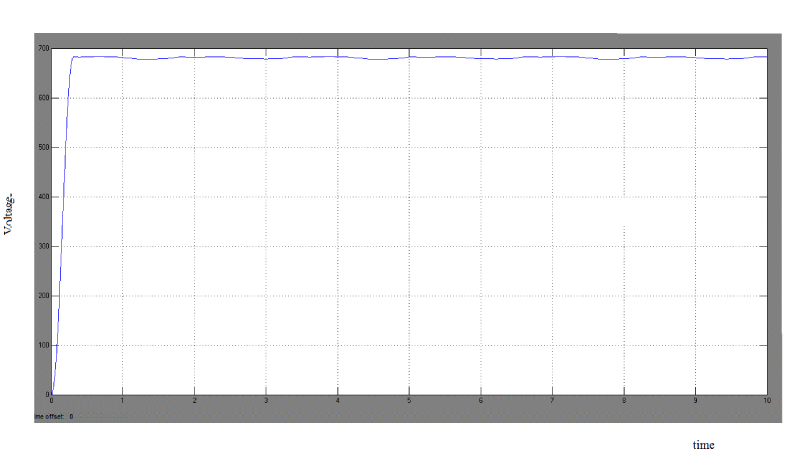
| The above Fig.6 shows the output voltage of modified sepic converter. During the voltage is regulated to 100V the PI controller will track the set point value. This PI will provide optimum convergence to the output value. |
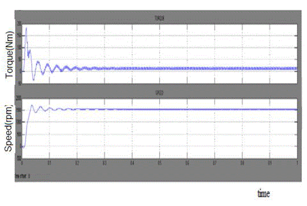
| The above Fig.7 shows that speed and torque of induction motor. When the Load regulated, line side power factor is maintained. |
CONCLUSION
|
| This Paper has presented a Bridgeless DCM SEPIC With PI Controller. Bridgeless SEPIC for power factor correction with low conduction losses and load regulation is done. The proposed topologies are designed to work in discontinuous conduction mode (DCM) to achieve almost unity power factor. The DCM operation gives additional advantages such as zero-current turn-on in the power switches, zero-current turn-off in the output diode and reduces the complexity of the control circuitry. The output to input relation is controlled by PI controller. The proportional controller checks the error between actual and reference voltage. The integral controller will compensate this error by comparing error with repeated sequence. The value again compared with PWM signal. The usage of PI controller will reduce the error between reference and actual value.DCM is preferred to produce almost unity power factor. When the Load regulated, line side power factor is maintained. The proposed converter is simulated by using MATLAB performance waveforms are verified. |
| |
Figures at a glance
|
 |
 |
 |
 |
| Figure 1 |
Figure 2 |
Figure 3 |
Figure 4 |
 |
 |
 |
| Figure 5 |
Figure 6 |
Figure 7 |
|
| |
References
|
- A.Bakhshai,P.Das,J.Drobnik,P.K.Jain,M.Pahlevaninezhad, and, “A novel ZVZCS full-bridge DC/DC converter used for electric vehicles,”IEEE Trans. Power Electron., vol. 27, no. 6,june 2012.
- A.Bakhsha,P.Das,J.Drobnik, P.K.Jain,M.Pahlevaninezhad,(2012) and, “A ZVS interleaved boost AC/DC converter used in plug-in electric vehicles,”IEEE Trans. Power Electron., vol. 27, no. 8,aug 2012.
- A.Bakhshai,J.Drobnik,P.K.Jain,andM.Pahlevaninezhad,(2012)“A loadadaptive control approach for a zero-voltage-switching DC/DC converter used for electric vehicles,”IEEE Trans. Ind. Electron., vol. 59.,aug 2012.
- AhmadJ.Sabzali,Esam,H.Ismail,Mustafa,A.AlSaffar,and Abbas A.Fardoun, “New Bridgeless DCM Sepic and Cuk PFC Rectifiers With Low Conduction and Switching Losses,” IEEE Trans. Ind. Electron vol. 47,no.2, pp.873-881, Jun 2011.
- E.H.Ismail,“Bridgeless SEPIC rectifier with unity power factor and reduced conduction losses,” IEEE Trans. Ind.Electron., vol. 56, no. 4,pp.= 1147–1157, Apr 2009.
- C.M Wang,“A novel single-stage high-power-factor electronic ballast with symmetrical half-bridge topology,”IEEE Trans. Ind. Electron.,vol. 55, no. 2, pp. 969–972, Feb 2008.
- P.Kong,S.Wang and F.C.Lee,“Common mode EMI noise suppression for bridgeless PFC converters,”IEEETrans.Power Electron., vol. 23,no. 1, pp. 291–297, Jan 2008.
- W.Y.Choi,J.M. Kwon and B.H. Kwon,“Bridgelessdualboost rectifier with reduced diode reverse-recovery problems for power-factor correction,”IET Power Electron., vol. 1, no.2, pp. 194–202, Jun. 2008.
- Y.Jang,M.M.Jovanovic and D.L.Dillman,“Bridgeless PFC boost rectifier with optimized magnetic utilization,” in Proc.IEEE Appl. PowerElectron. Conf. Expo., 2008, pp. 1017–1021.
- L.Huber,Y.Jang, and M. M. Jovanovic,“Performance evaluation of bridgeless PFC boost rectifiers,” IEEE Trans.Power Electron., vol. 23,no. 3, pp. 1381–1390, May 2008.
- W.WeiL.Hongpeng,J.Shigong, and X.Dianguo,“A novel bridgeless buck-boost PFC converter,” in Proc.IEEE Power Electron. Spec. Conf., 2008, pp. 1304–1308.
- H.Y.Tsai, T.H.Hsia and D.Chen,“A novel soft-switching bridgeless power factor correction circuit,” in Proc. Eur.Conf. Power Electron. Appl., 2007, pp. 1–10.
- W.Y.Choi,J.M.Kwon,E.H.Kim,J.J.Lee,B.H.Kwon,“Bridgeless boost rectifier with low conduction losses and reduced diodereverse-recovery problems,”IEEETrans.Ind. Electron., vol. 54, no. 2,pp. 769–780, Apr. 2007.
- X.Xin,T.Liu,J.Zeng,H.WuJ.Ying,“Asymmetrical HPFC for low line applications,” in Proc. IEEE Power Electron. Spec. Conf., 2007, pp. 1077– 1081.
- J.C.Liu,C.K.Tse,N.K.Poon,B.M.Pong and Y.M.Lai, “A PFC voltage regulator with low input current distortion derived from a rectifierless topology,” IEEE Trans. Power Electron.,vol. 21, no. 4, pp. 906–911,Jul. 2006.
- C.M.Wang,“A novel zero-voltage-switching PWM boost rectifier with high power factor and low conduction losses,”IEEE Trans. Ind. Electron.,vol. 52, no. 2, pp. 427–435, Apr. 2005.
- H.Ye,Z.Yang,J.Dai,C.Yan,X.Xin,andJ.Ying,“Common mode noise modeling and analysis of dual boost PFCcircuit,”in Proc.Int. Telecommun. Energy Conf., 2004, pp. 575–582.
- T.Ernö and M.Frisch,“Second generation of PFC solutions,”Power Electron. Eur.,no. 7, pp. 33–35, 2004.
- G.Moschopoulos and P.Jain,“A novel single-phase softswitched rectifier with unity power factor and minimal component count,” IEEE Trans.Ind. Electron, vol. 51, no. 3,pp. 566–576, Jun. 2004.
- U.Moriconi, “A bridgeless PFC configuration based on L4981 PFC controller,” Appl. Note AN1606, STMicroelectron,Geneva, Switzerland,Nov. 2002.
|