Keywords
|
| PID controller, Pulse Width Modulation (PWM), Sliding mode control, DC-DC buck converter, Transfer function, MATLAB, Simulink |
INTRODUCTION
|
| The switch mode DC-DC converter are some of the simplest circuit which converts power level of DC power effectively. It has wide application in modern computer, DC motor drive, power system, automotive, aircrafts etc. the commonly used control methods are pulse width modulation (PWM), voltage mode control, PWM current mode control with proportional (P), proportional integral (PI), and proportional integral derivative (PID) controller. But this control method cannot perform satisfactory under large load variation so non liner control technique is in picture.The dc-dc converters, which are non-linear and time variant system, and do not lend themselves to the application of linear control theory, can be controlled by means of sliding-mode (SM) control, Which is derived from the variable structure control system theory (VSCS). |
LITEARTURE SURVEY
|
| The dc-dc switching converters are the widely used circuits in electronics systems. They are usually used to obtain a stabilized output voltage from a given input DC voltage which is lower (buck) from that input voltage, or higher (boost) or generic (buck–boost) [1]. Most used technique to control switching power supplies is Pulse-width Modulation (PWM) [2]. The conventional PWM controlled power electronics circuits are modelled based on averaging technique and the system being controlled operates optimally only for a specific condition [3]-[4]. The linear controllers like P, PI, and PID do not offer a good large-signal transient (i.e. large-signal operating conditions) [4]-[5]. |
| Therefore, research has been performed for investigating non-linear controllers. The main advantages of these controllers are their ability to react immediately to a transient condition. The different types of non-linear analog controllers are: (a) hysteretic current-mode controllers, (b) hysteretic voltage-mode/V2 controllers, (c) slidingmode/ boundary controllers. Advantages of hysteretic control approach include simplicity in design and do not require feedback loop compensation circuit. M. Castilla [6]-[8] proposed voltage-mode hysteretic controllers for synchronous buck converter used for many applications. The analysis and design of a hysteretic PWM controller with improved transient response have been proposed for buck converter in 2004[9]. |
BASIC PRINCIPLES
|
| The buck converter circuit converts a higher dc input voltage to lower dc output voltage. The basic buck dc-dc converter topology is shown in figure. 1. It consists of a controlled switch Sw, an uncontrolled switch (diode) D, an inductor L, a capacitor C, and a load resistance R. |
| In the description of converter operation, it is assumed that all the components are ideal and also the converter operates in CCM. In CCM operation, the inductor current flows continuously over one switching period. The switch is either on or off according to the switching function and this results in two circuit states. The first sub-circuit state is when the switch is turned on, diode is reverse biased and inductor current flows through the switch, which can be shown in figure 2(a). The second sub-circuit state is when the switch is turned off and current freewheels through the diode, which is shown figure 2(b). |
| The basic idea of SM control is to design first a sliding surface in state space and then the second is to design a control law direct the system state trajectory starting from any arbitrary initial state to reach the sliding surface in finite time, and finally it should come to a point where the system equilibrium state exists that is in the origin point of the phase plane. The existence, stability and hitting condition are the three factors for the stability of sliding mode control. SM |
| control principle is graphically represented in Figure 3, where, represent the sliding surface and x1 and x2 are the voltage error variable and voltage error dynamics respectively. The sliding line (when it is a two variable SM control system in two-dimensional plane) divides the phase plane into two regions. Each region is specified with a switching state and when the trajectory arrives at the system equilibrium point, the system is considered as stable. |
IMPLEMENTATION OF PID CONTROLLED BUCK CONVERTER
|
| The simulation model of DC-DC buck converter consists of following parts: |
| DC-DC Buck Converter: ADC-DC buck converter is a power electronics device to convert high level of voltage to a lower level voltage. In this paper the buck converter is implemented in two forms. One is mathematical modelling and another is electrical modelling. A buck converter is consists of Inductance (L), Inductance Series Resistance (RL), Capacitance (C), and Capacitance Series Resistance (Rc). |
| The mathematical model of the system consists of two loop. 1st one is inductor current and 2nd is output voltage loop. To design this two loop general equation must have to derive from variable system structure model. |
| From the general model of buck converter we can assume: |
| The first loop is responsible for computing the Inductor current by solving the differential equation obtained from applying KVL |
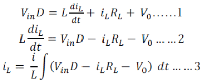 |
| Where, Vin= Input Voltage of the Buck Converter, D=1 when Duty Cycle is ON and D=0 when Duty Cycle is OFF, iL= Inductor Current, RL=Effective Series Resistance of Inductance, V0=Output Voltage of the Buck Converter, L=Inductance Value in Henry. |
| The second loop calculates the Output Voltage which is the sum of the Capacitor Voltage and the drop across the Capacitor Series Resistance (Rc). Applying KCL at the capacitor node we get: |
 |
| Where iout = Load Current, C = Capacitance in Farad, Vc=Voltage across Capacitor, RC = Effective Series resistance of the Capacitor. |
| PWM generator: The PWM generator produce switching frequency for the desire output by varying the duty cycle of the converter. The converter has two operating mode. The duty interval, when switch is on (Ton) and freewheeling mode, when switch is off (Toff). |
| To implement a PWM subsystem a relay is necessary to provide output. The input of the relay is the difference of duty cycle and saw tooth waveform. By varying the duty cycle the turn off and turn on period varies. With that the output of the relay also changes. A very simple PWM generator is designed in this paper. The time value of saw tooth is [0 0.1/fs], where fs is switching frequency. The only relay parameter ‘output when on’ value is 1 rest of that all value is 0. |
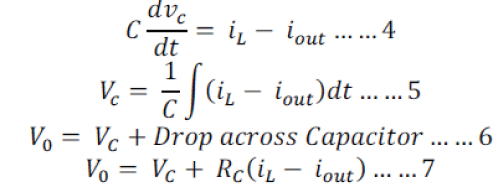
| PID Controller: To design a PID controller successfully first have to design a transfer function of the system with respect to duty cycle. |
| By applying Laplace Transform to Eqn (2), we get: |
 |
| Let us assume Vc=V0 by neglecting the drop across Rc. Using Laplace Transform on Eqn (9) and rearranging the terms, we get |
 |
| By substituting the value of iL in Equation (10) and rearranging the terms, we obtain the open loop transfer function of the Buck Converter: |
 |
| By applying different tuning technique like Ziegler– Nichols, Cohen–Coon the value of Kp, Kd, Ki can be derived for the system. |
| The proposed system is as follows: |
| The parameters of the model is input voltage Vin = 24 volt, reference voltage Vref = 18 volt, inductance L = 0.001H, capacitance C = 0.75μC, leakage inductance RL = 0.08 Ω, leakage capacitance RC = 0.03 Ω. |
| In this model of buck converter the reference voltage Vref is 18 volt constant supply. The load resistance is 10 Ω. Input voltage of the converter is Vin is 24 volt dc supply. The output voltage of this converter is Vout and it is 17.66 volt and current Iout 1.794 amp. Both are rippled and fluctuating but magnitude is moderate. |
SLIDING MODE CONTROL FOR BUCK CONVERTER
|
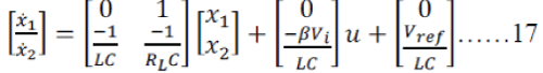
| To design a sliding mode controller for Buck converter, the voltage error, X1, is |
 |
| Where Vref is the constant reference voltage and β = R2/ (R1 + R2) is the sensing ratio of the output voltage. The rate of change of voltage error, X2, is |
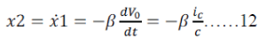 |
| Where IC = C (dVo/dt) is the capacitor current, and C is the capacitance. Since IC = IL − IR, where IL and IR represent the inductor and load currents respectively, differentiation of above equation with respect to time gives |
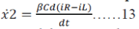 |
| Using IR = Vo/RL where RL is the load resistance, and the averaged equation of a CCM inductor current |
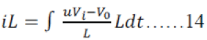 |
| Where Vi is the input voltage, L is the inductance, and u = 1 or 0 is the switching state, we have |
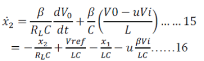 |
| Finally, from (4.4) and (4.6), a state space model describing the system is derived as |
 |
| The proposed model for buck converter is as follows: |
RESULT AND DISCUSSION
|
| The model is verified in MATLAB/ Simulink environment. The input voltage of the buck converter is Vin 24 volt DC load is 10Ω. The reference signal of the system is Vref 18 volt DC. The output voltage Vout 17.89 volt shown in fig 13 (a). The rise time of the system is 0.1 sec and no overshoot in the output voltage. |
| The output current waveform is in the next figure 13 (b). The value of output current is 1.764 amp. The settling time is 0.08 second. |
| The control methods have the same power circuit parameters and operate at the same input and output voltages. The design specifications and the circuit parameters, for simulation are chosen as: input voltage Vin =24V, desired output voltage Vout =18V, inductance L =100mH, capacitance =150μF, leakage inductance RL= 0.08 Ω, leakage capacitance RC = 0.03Ω load resistance R =10Ω. The sliding coefficients =0.167. The switching frequency is set to 150 kHz. The output is Vout = 17.97 volt Io = 1.764 amp. |
CONCLUSION
|
| In this section Sliding Mode control of buck converter is implemented and different output parameter is observed. The output voltage and current is stable and satisfactory. The output is better than the PID control buck converter. Output reaches stability quite fast and ripple is minimum. Load variation up to a certain range does not affect the output. The overall performance of nonlinear control is good as compared to the PID controller. PID controller reaches its final value faster but contains ripple. For different load and PID parameters there overshoot may be seen. But in SM control the output is smooth and no overshoot observed. |
| |
Figures at a glance
|
 |
 |
 |
 |
 |
| Figure 1 |
Figure 2 |
Figure 3 |
Figure 4 |
Figure 5 |
 |
 |
 |
 |
 |
| Figure 6 |
Figure 7 |
Figure 8 |
Figure 9 |
Figure 10 |
 |
 |
 |
| Figure 11 |
Figure 12 |
Figure 13 |
|
| |
References
|
- M. H. Rashid, Power Electronics: Circuits, Devices and Applications (3rd Edition), Prentice Hall, 2003.
- N. Mohan, T. M. Undeland, W. P. Robbins, “Power Electronics: Converters, Applications, and Design”, 3rd Bk&Cdr edition, Wiley, 2002.
- R.D Middlebrook and S Cuk , “A general unified approach to modelling switching Converter Power stages”, in Proc. IEEE PESC Rec., pp. 18– 34, 1976.
- A.J. Forsyth and S.V. Mollow, “Modellingand control of dc-dc converters”,IEE power engineering journal, vol. 12, no. 5, pp. 229–236, Oct. 1998.
- V.S.C Raviraj and P.C. Sen, “Comparative Study of proportional-integral, Sliding-mode, and fuzzy logic controllers for power converters”,IEEEtransaction on Industry applications, vol. 33, no. 2, pp. 518-524, Mar. /Apr. 1997.
- M. Castilla, L. G. de Vicuna, J.M. Guerrero, J. Matas, and J. Miret, “Design of voltage-mode hysteretic controllers for synchronous buck converters supplying microprocessor loads”, IEE Proceedings on Electrical Power Applications, Vol.152, No. 5, pp.1171–1178, Sep. 2005.
- M. Castilla, L. G. de Vicuna, J.M. Guerrero, J. Miret, and N. Berbel, “Simple low-cost hysteretic controller for single-phase synchronous buck converter”, IEEE Transactions on Power Electronics, Vol. 22, No. 4, pp.1232–1241, Jul. 2007.
- 8.M. Castilla, L. G. de Vicuna, J.M. Guerrero, J. Matas, and J. Miret, “Designing VRM hysteretic controllers for optimal transient response”, IEEE Transactions on Industrial Electronics, Vol. 54, No. 3, pp.1726–1738, Jun. 2007.
- T. Nabeshima, T. Sato, S. Yoshida, S. Chiba, and K. Onda, “Analysis and design considerations of a buck converter with a hysteretic PWM controller”, in Proc. IEEE PESC, pp. 1711–1716, 2004.
|