Many of the present communication systems tend to use Orthogonal Frequency Division Multiplexing (OFDM) because of the higher data rates, low inter symbol interference (ISI) and easily compatible to the variation in the frequency. The present standards use inbuilt IP’s for the implementation of OFDM Transmitter and Receiver. This work provides the validation and implementation of OFDM Transceiver on FPGA which is completely digital, and the whole work is done using VHDL language. Field Programmable Gate Arrays provide the better platform for the variation of data rates and moreover they are of low cost, easily programmable. Software tools and hardware used in the implementation are Xilinx ISE, Modelsim, Chipscope tools and Spartan 3E FPGA
Keywords |
| OFDM, FPGA, Xilinx ISE, Modelsim , Chipscope |
INTRODUCTION |
| In some applications, it is desirable to transmit the same information-bearing signal over several channels. This mode
of transmission is used primarily in situations where there is high probability that one or more of the channels will be
unreliable from time to time. One form of this multichannel signaling is sometimes employed in wireless
communications systems as means of overcoming the effects of interference of the transmitted signal. By transmitting
the same information over multiple-channels, provides signal diversity, which the receiver can exploit to recover the
information. Another form of the multichannel communications in multiple carrier transmission, where the frequency
band of the channel is subdivided into a number of sub-channels and information is transmitted on each of the subchannels.
In non-ideal linear filter channels it is observed that such channels introduce ISI, which degrades
performance compared with the idea channel. The degree of performance degradation depends on the frequencyresponse
characteristics. Furthermore, the complexity of the receiver increases as the span of ISI increases. In this
system, we consider the transmission of information on multiple carriers contained within the allocated channel
bandwidth. The primary motivation for transmitting data on multiple carriers is to reduce ISI and thus, eliminate the
performance degradation that is incurred in several methods to implement the system. One of such methods of
implementing this system is by using FPGA (Field Programmable Gate Array). |
| OFDM, carried out in digital domain on FPGA, which is a programmable hardware and the full control over the actual
design implementation resides with the user and there is no need for any physical IC fabrication facility. An FPGA with
the programmability of a general purpose processor combines the speed, power and density attributes. This will be
advantageous to the OFDM system implementation. To meet the future needs new functions should be added to the
existing model and for this implementation FPGA is the better platform and can be easily fabricated to a chip. Thereby
FPGA will be a good platform than any other for the OFDM implementation since it gives flexibility t the program
design besides the low cost hardware component comparing to others. |
PRINCIPLES OF OFDM |
| Multicarrier modulation divides the available channel bandwidth into sub-bands of relatively narrow width (/\f), which
provides a solution that could yield transmission rates close to channel capacity. The signal in each sub band may be
independently coded and modulated at a synchronous symbol rate of (1/( /\f)).If width is small enough, the channel
frequency response is essentially constant across each sub-band. Hence, the inter symbol interference is negligible.
Here comes the concept of OFDM where the symbol rate selected in each of the sub-channels is equal to the frequency
separation of the adjacent sub-carriers, the sub-carriers are orthogonal over symbol interval, independent of the relative phase relationship between the sub-carriers. OFDM is widely used in both wire-line and radio channels. OFDM has
been adopted as a standard for digital audio broadcast applications and wireless local area networks based on IEEE
802.11 standard. OFDM, a special case of multi-carrier transmission is a technique in which single stream of data is
transmitted over a number of lower rates sub-carriers. In general FDM (frequency division multiplexing) the total band
is divided into non overlapping frequency channels. Literally speaking, same is the case with the OFDM, but in here
the total band is divided in a number of orthogonal sub-carriers, which results in the better use of spectrum. An OFDM
system mainly consists of a modulator, serial to parallel converter, IFFT, FFT, parallel to serial converter,
demodulator. The FFT’s iterative nature and the computational order make OFDM ideal for dedicated architecture. |
| To overcome the errors during the transmission of signal, forward error correction is applied to the signal before
transmission and this concept is called COFDM(Coded Orthogonal Frequency Division Multiplexing).This will
overcome errors in the transmission due to lost carriers from frequency selective fading, noise and interference.
Typically 10 kHz – 30 kHz bandwidth is made available for each user in FDMA, to transmit all the user information.
This allocated bandwidth is wider than the required speech bandwidth which is 3 kHz to prevent the interference. In
this process 50% of the total spectrum goes of no use and this gets worse as the channel band-width becomes narrower,
and also with increase in the frequency band. In QPSK modulation, user requires a band-width of 2-7 kHz , but FDMA
isn’t that god to handle such band-width, here comes the TDMA into picture , which uses wider band-width channels.
Multiple users can handle same frequency at different time slots. Thereby, many low data rate users can be combined
together to transmit in a single channel, and so the spectrum can be used efficiently. However there are some problems
with TDMA. An overhead is to be added to the each packet of data which contains the source address and the
destination address. Due to the delay variations and synchronization errors change over time must be allocated to allow
for any tolerance in the start time of each user, which limits to the definite number of users. |
| TDMA has a problem with the high symbol-rate causing multiple path delay spread. OFDM overcomes most of the
problems. In OFDM the sub-carriers are placed close to each other and there is no requirement of overheads because
each user has one channel and the channels are integer number multiples of the symbol-period resulting in the
orthogonality among the carriers, which results in no inter-symbol interference between the carriers and spacing them
as closely as possible. Finally, each carrier in an OFDM signal has a very narrow band-width (approx. 1 kHz), resulting
in high tolerance to multipath delay spread. |
IMPLEMENTATION OF OFDM TRANSCEIVER |
A. OFDM TRANSMITTER BLOCKS |
| 1) Input Sampler: The input sampler is the first block of the OFDM transmitter section. Serial data is fed as input to the
block, and the output is a 2-bit IQ. The output is group of symbols, each containing two bits. So this input sampler is
the block which groups two bits. |
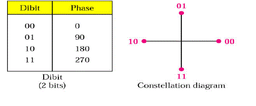
| 2) SYMBOL MAPPER: The output of the input sampler is fed as input to the symbol mapper. The symbol mapper
consists of an QPSK modulator. The input 2-bit stream fed to the modulator divides it into two 2-bit symbols called I
and Q (imaginary and quadrature). These symbols are generated based on the constellation diagram. In QPSK there are
four phases, each 2-bit symbol is assigned to a phase, which are of 90 degrees difference between them. The coding is
done based on the constellation diagram of QPSK |
| 3) SERIAL INPUT PARALLEL OUTPUT (SIPO): This block’s input is the output from the symbol mapper. SIPO, as
the name indicates serial input parallel output, this block converts the serial data fed as input to parallel data. In this
system, SIPO is a two 8 register (0-7) array. The serial input is fed at the seventh array and for every clock cycle the
data is shifted to the above register. After 8 clock cycles the data in the array is forwarded. The SIPO output contains 8
registers of real data and remaining eight imaginary 8 data registers. |
| 4) INVERSE FAST FOURIER TRANSFORM (IFFT): It is the most important module of the OFDM system. The IFFT
input will the output from the SIPO. In this system, we require 2 IFFT modules, one for the real and the other for
imaginary. The IFFT converts frequency domain constraints to time domain. The time domain values are transmitted as
OFDM signals through the transmitter. In this system, IFFT is performed in steps. At first exchange real and imaginary
parts, perform FFT, exchange the real and imaginary parts, and finally divide with N, which is the number of inputs
fed, here it is 8. At, last we have the time domain values which are transmitted through the transmitter. |
B. OFDM RECEIVER BLOCKS |
| 1) FAST FOURIER TRANSFORM (FFT): In the receiver section, this is the main module. OFDM signals are received
from the antenna and are fed to the FFT, which converts them back to frequency domain. In this system, Decimation in
frequency (DIF)-FFT is used. The Fast Fourier Transform (FFT) transforms a cyclic time domain signal into its
equivalent frequency spectrum. This is done by finding the equivalent waveform, generated by a sum of orthogonal
sinusoidal components. The amplitude and phase of the sinusoidal components represent the frequency spectrum of the
time domain signal. |
| 2) PARALLEL INPUT AND SERIAL OUTPUT (PISO): A parallel to serial converter is a special function of a shift
register. The data is loaded parallel into the shift register and then shifted bit by bit. In this system, this bock is used to
convert the data obtained from the FFT into serial data and is fed as input to the symbol demapper ,The converter has to
wait up to 8 cycles for the next data to be loaded |
| 3) SYMBOL DEMAPPER: Input to this bock is fed from the PISO, from the received real and imaginary parts, based on
fixed threshold level, which is of half the amplitude of the input signal, comparing the threshold value with the
received input signal, the output is determined. This is the concept behind the QPSK demodulator |
| 4) OUTPUT BIT GENERATOR: This block takes 2 bit IQ from Symbol demapper and generates output bits. This
consists of a shift register of 2 bit length, for every clock cycle data is entered, shifted and exited. |
IMPLEMENTATION RESULTS |
| The work presented in this paper aimed in demonstrating the capability of a straight forward translation of wireless
communication system into a pure VHDL implementation on reconfigurable platform. The work has accomplished the
task of designing the digital baseband part of an OFDM transceiver. Results are driven for the transmitter block using
Xilinx. Codes are completely in the VHDL language. |
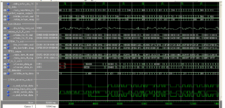
| The last two results represents the input fed to the OFDM transmitter and the output from the OFDM receiver, the
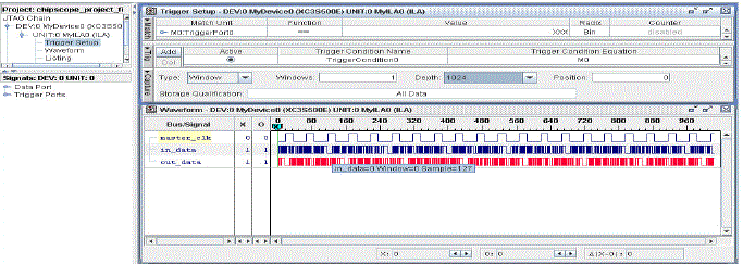
signals are same with delay. These are the simulation from the Modelsim. Now the code is dumped into Spartan 3E
FPGA kit and the results observed on Chipscope with input, clock and output as the signals. The result of the
Chipscope is |
CONCLUSION |
| A baseband OFDM transmitter and receiver were successfully designed. Each block was tested using Xilinx ISE. The
complete resource utilization is 4% f the number of slice FLIP FLOPS and 72% of 4 input LUT’s |
| |
Figures at a glance |
 |
 |
 |
 |
 |
| Figure 1 |
Figure 2 |
Figure 3 |
Figure 4 |
Figure 5 |
|
| |
References |
- Lenin Gopal, Daniel Wong âÃâ¬ÃÅDesign of an FPGA-Based OFDM Transceiver for DVB-T StandardâÃâ¬Ã IEEE 978-1 4244-8728-8/11@2011.
- S.J. Vaughan-Nichols,âÃâ¬Ã OFDM: Back to the Wireless FutureâÃâ¬Ã IEEE Computer, pp.Vol-II 19-21.2002
- AnupamaKamboj, ShivaniSehgal, âÃâ¬ÃÅDesign of baseband OFDM TransmitterâÃâ¬Ã IJERT ISSN: 2278-0181 Vol. 1 Issue6,2012.
- SuranjanaJulis, AnhDinh, Fixed Point Design and Implementation of OFDM TransmitterâÃâ¬Ã Proceedings of World Congress on Engineering and Computer Science Vol. II. 2011
- Sghaier, S. Areibi, B. Dony, âÃâ¬ÃÂA Pipelined implementation of OFDM Transceiver on Reconfigurable platformsâÃâ¬Ãâ¢, CCECE 2008,Proc. Of the 2008 CCECE, pp. 8801-804, May. 2008
- C.Dick and F.Harris, âÃâ¬ÃÅFPGA Impementation of an OFDM PHYâÃâ¬Ã Signals, Systems and computers,2003,Conference record of the Thirty-seventh Asiomar Conference,vol.1, pp 905-909, Nov 2003.
- Y.Kim, H. Jung, H. HoLeeâÃâ¬Ã MAC Implementation for IEEE 802.11 Wireless LAN) and High Speed Intelligent Internet Symposium.âÃâ¬ÃÂ, ATM(ICTAM 2001
|