Keywords
|
| Register transfer level, Reduced instruction set computer(RISC), Very high speed integrated circuit(VHSIC) hardware description language , Arithmetic logic unit(ALU), Field programmable gate array(FPGA). |
LITEARTURE SURVEY
|
| Since the programmable logic technology has been developed highly. It has become feasible that the processors based on FPGA are implemented in the laboratory. Several soft processor cores are being available now days, such as Xilinx, Pico Blaze, Altera Nios. But these processor cores are being provided as black boxes or black box units in which case a user is just unable to monitor internal signals, and the operation process, neither can modify the original structure. FPGAs have especially led to the development of designs in high level description languages like VHDL or Verilog ,which allow the designer to conceive the design at the level of RTL without reference to the final technology or vendor used for the final implementation.[1] |
| VHDL is an efficient programming language that allows one to model easily and develop complex digital systems in a dynamic hardware description language..The authors in [2] proposed a VHDL based rapid prototype approach to simulate ,synthesize and implement a computer system using commercial CAD tools. The usage of VHDL for the designing and implementation of a CPU structure has been presented in[3]. In the design implementation of 16 bit CPU [4], the author has obtained the minimum clock period of 31.46ns and with the proposed design architecture, the clock period is highly reduced as shown in the simulation results , so that fast processing can be achieved. |
INTRODUCTION
|
| The requirements for the language were being first generated in 1980s, under the title Very High Speed Integrated Circuit (VHSIC) project of US government, in order to enhance the electronic technology, design process, and procurement, as well as the development of many advanced IC process technologies. Any hardware design can be described in terms of its operations at different levels of abstraction, from system through to logic gates. At each level of this hierarchy the overall inputs and outputs remain the same but the functionality of distinct sections become clearer with the help of detailed schematics |
| IC design indulges in more complex computations as compare with the software version and found to be time consuming .The design needed to develop such as microprocessor of required specification by conventional approach will lead to reduction in machine cycle, variation in data bus size, reduction in cost, and implementation of all numbering system. After implementing such a system, major questions raises in the shape of its integration and optimization. These problems have been eliminated by Field Programmable Gate Array (FPGA) technology and by Hardware Descriptive Language(HDL).The software interface along with chip design and planner reduces the complexity and enhances the ease of computations .[5],[6],[7]. |
| With the proposed design in this paper, the 64 KB memory is interfaced with the CPU and the minimised delay, clock period, path delay are obtained. The proposed design has been tested with some application programs of memoryrelated operations (load, store, move, and branch). |
TECHNICAL WORK PREPARATION
|
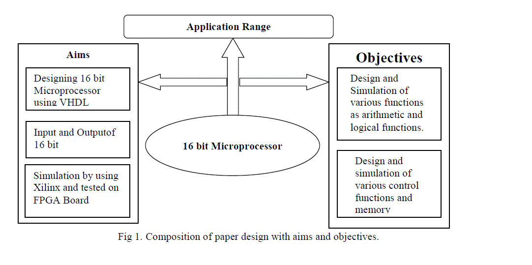
| Various tools are put forth in designing of this system. In the present case microprocessor is bricked up using synthesized operations in the form of objectives and broader aspects. Fig. 1.shows the organization of the paper design that is needed to implement: |
a) System overview
|
| This paper design has been represented by separate modules. The main focus amongst them for Operational Design , Software Design and Hardware Design. |
Operational overview
|
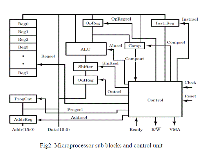
| The operational view deals with various kinds of operation which a microprocessor can perform. The CPU (Central Processing Unit) is the “brain” of computer. It is composed of several parts , like data path, control path and memory units. At each clock cycle, Control Unit is needed to generate the control signals automatically for operating the data path. It is based on the finite state machine concept. The control unit for a processor basically cycles through three main steps, usually referred to as the instruction cycle i.e Fetch an instruction, Decodes the instruction and Executes the instruction. Second part deals with the Arithmetic Logic Unit which perform arithmetic computations such as addition ,subtraction, multiplication, division, increment, decrement and logical functions such as AND ,OR , XOR ,left shift ,right shift etc [7]. |
Software overview
|
| Interfacing with VHDL software used in this system, reduces the complexity and also provide the graphic presentation of the system.VHDL is advantageous when used for systems design is that it allows the behavior of the required system to be described(modeled) and verified (simulated) before synthesis tools translate the design into real hardware (gates and wires).This not only indulge in compilation but also produces waveform results. For performing compilation and simulation of any logic circuit design, few sophisticated Computer Aided Design(CAD) tools such as Alteras II and Xilinx web pack are used [10]. |
Hardware overview
|
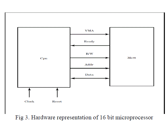
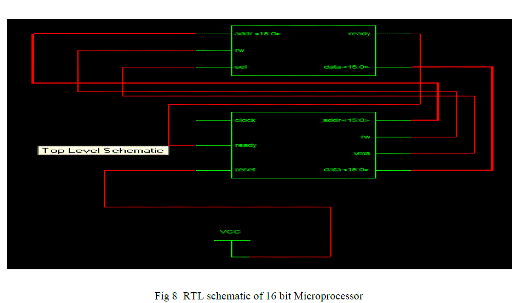
| The Fundamental building block of microprocessor is shown in fig 3. This model instantiates components cpu and mem and specifies the necessary signals to connect the components, as shown in figure below. |
| Component mem is a memory device and contains the instructions and data for the CPU to execute. Component cpu is an RTL implementation of the CPU device that is simulated for correctness and synthesized to implement the design. It includes clock signal ,reset valid memory address(VMA),address register,ready signal and data is required for operation.A final point is that when a VHDL model [11] is translated into the "gates and wires" that are mapped onto a programmable logic device such as a CPLD or FPGA, and then it is the actual hardware being configured, rather than the VHDL code being "executed" as if on some form of a processor chip. |
| Instruction register is for storing the instruction being fetched from the memory. The program counter holds the address of the memory of the current instruction. After the execution of instruction, the program counter move to the next instruction. If there is branch instruction, the program counter is loaded with the address of the next instruction . Then the value of the program counter is copied by the control unit to the address register, which gives the new address in address bus .The process of storing data into memory is called writing and retrieving data or opcode from the memory is called reading. |
EXPERIMENTAL RESULTS
|
| Synthesis and simulation of the VHDL code of the processor using Xilinx Software (Version 9.1) is presented. The synthesis and simulation results are presented for justification .Using Xilinx ISE 9.1 software the code is tested and checked. The simulation results are compared with the theoretical results. Before the start of simulation, the instructions and data are written and loaded into the memory. The processor with memory is tested for arithmetic and logical operations . When the VHDL code is fully synthesized, then the code is loaded to the Spartan FPGA device[8]. |
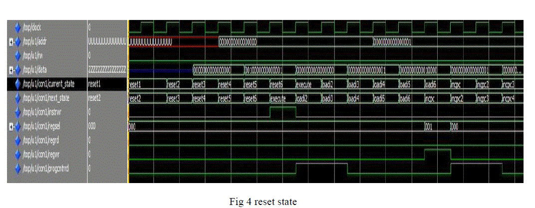
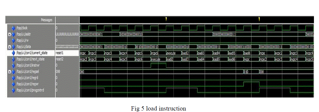
| This state executes according to the state machine modelling as the sequential process sets signal current_state to state value reset1. This is the first state of the reset sequence for the CPU which starts the process of getting the CPU ready to execute instructions. the CPU ready to execute instructions .If the reset signal is not ‘1’ and there is a rising edge on the clock signal, then the next state signal generated by the combinational process is copied to signal current _state. This is the method for the state machine to advance from one state to another. After the reset signal is set to a value other than ‘1’, the state machine is in state reset1. Moving further control passes to state reset 2,reset3,reset 4,reset 5 and finally goes to reset 6 and, depending on the value of the ready signal from the memory, either stays in reset6 or writes the memory data value to register InstrReg and goes to state execute. |
| At this point, the state machine has reset the state of the CPU to a known state and loaded the first instruction into register InstrReg. From this point forward, the state machine changes state depending on the instructions encountered. |
| In the above figure, the load instruction is executed. With the help of this instruction the data is loaded from the external memory to the microprocessor. The load instruction can be immediate where the data to be loaded is the part of the instruction .The load instruction is executed in the state machine manner where the current state starts from load 1 and end at load 6. |
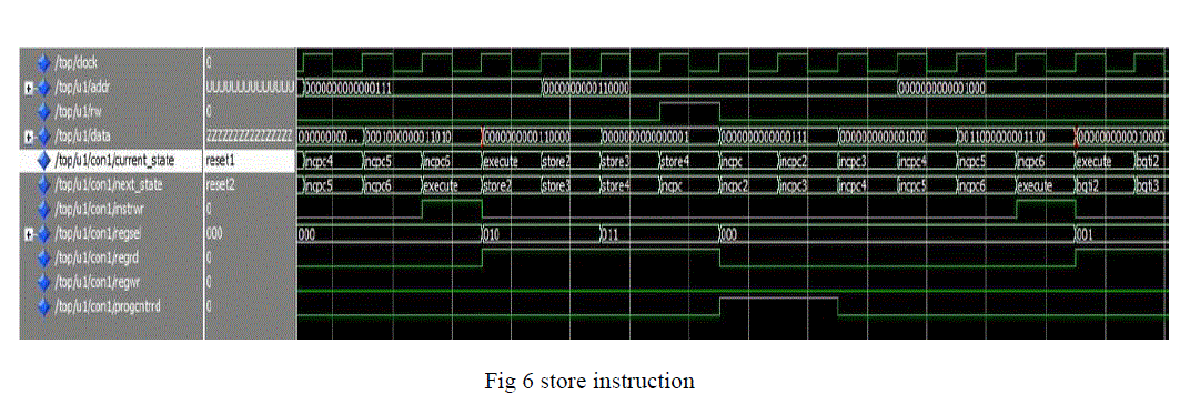
| In the above figure ,the store instruction is executed. With the help of this instruction the data is loaded from the microprocessor to the external memory. |
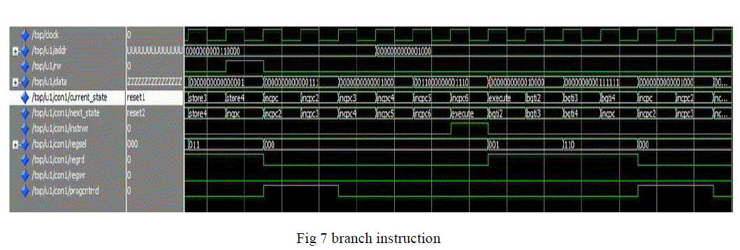
| In this execution, the data is compared with the defined value and if the condition is true, the control jumps to the defined label(address) and if the condition become false, the next instruction is executed. |
ANALYSIS REPORTS
|
| Following analysis reports are obtained using Xilinx ise 9.2i for synthesis and map reports: |
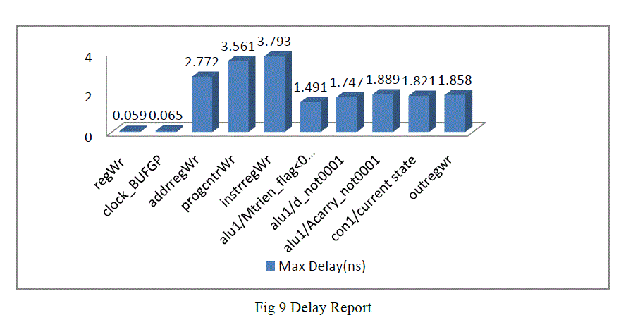
| This figure shows the maximum delay operation of each module of microprocessor during the execution of whole operation. |
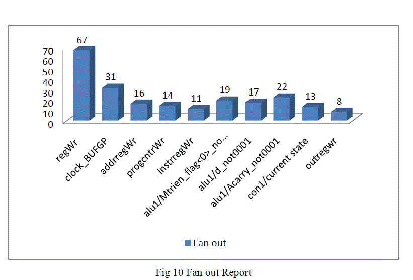
| As we know that fan out is the greatest number of input of gates of same type to which the output can be safely connected .Fan out of logic gate output is number of gate inputs, it can feed or connect to. The maximum fan out of output measures it’s load driving capability. |
| The synthesis report include total number of slices, LUT, Input, Output blocks and buffers. LUT: A logic cell consist of a look up table , flip flop and connection to adjacent cells. The LUT uses combinational logic to implement a 4 i/p expression. |
| SLICES: A logic slice consist of two logic cell. A configurable logic block consist of 4 slices. This combine architecture gives benefits in final system such as increased performance of logic execution. |
CONCLUSION
|
| Some additional features in CPU have been added like complex addition ,complex multiplication and other logical operation etc. Some other modules can be added like timer , counter ,interrupt in this which can enhance the features of the processor .Since this processor is 16 bit so it is capable of accessing 16kb of external memory. More number of input output devices can be accessed simultaneously. |
Tables at a glance
|
 |
| Table 1 |
|
| |
Figures at a glance
|
 |
 |
 |
 |
 |
| Figure 1 |
Figure 2 |
Figure 3 |
Figure 4 |
Figure 5 |
 |
 |
 |
 |
 |
| Figure 6 |
Figure 7 |
Figure 8 |
Figure 9 |
Figure 10 |
|
| |
References
|
- Jurado-Carmona, F.J., Tombs, J., Aguirre, M.A., Torralba, A., “Implementation of a fully pipelined ARM compatible microprocessor core” XVII
- Hamblen J. “Using Synthesis, Simulation, and Hardware Emulation to Prototype a Pipelined RISC Computer System”. Atlanta, Georgia.
- Zainalabedin N.” Using VHDL for Modeling and Design of Processing Units”.Pp.315- 326, Boston, Massachusetts.
- ManoranjanPradhan,” Simulation and Verification of Self Test 16-Bit Processor”, International Journal of Computer Applications (0975 – 8887) Volume 20– No.1, pp.42-45,April 2011.
- Davidson, J. “FPGA Implementation of a Reconfigurable Microprocessor” IEEE Custom Integrated Circuits Conference, 1993, pp. 3.2.1- 3.2.4
- Sueyoshi, T., Kuga, M., and Shibamura, H.,“KITE Microprocessor and CAE for Computer Science”, Systems and Computers in Japan, Vol. 33, No. 8, 2002, pp.64-74.
- Pastor, J. S., Gonzalez, I., Lopez, J., Arribas ,F.G, Martinez, J. “A Remote Laboratory for Debugging FPGA-Based Microprocessor Prototypes” ,Proceedings of the IEEE International Conference on Advanced Learning Technologies (ICALT’04),2004.
- S. Kaliamurthy , R .Muralidharan , “VHDL Design of FPGA Arithmetic Processor” International Conference on Engineering and ICT, 2007.
- Allen Dewey, “Analysis and design of digital system with VHDL”, PWS publishing company, 1997.
- Data sheet of Spartan-II 2.5 FPGA Family. 2003. XILINX, DS001-2 (V2.2).
- Weijun Z. 2001. VHDL Tutorial, Learn by Example.
|