ISSN ONLINE(2319-8753)PRINT(2347-6710)
ISSN ONLINE(2319-8753)PRINT(2347-6710)
Julie Thomas#1, Selvaraj A*2
|
| Related article at Pubmed, Scholar Google |
Visit for more related articles at International Journal of Innovative Research in Science, Engineering and Technology
AC Adjustable Speed Drives (ASD’s) have become very popular variable speed control devices used in industrial, commercial and some residential applications. Modern solid state induction motor drives are highly sensitive to voltage sags. A voltage Sag is defined as a momentary decrease in the rms voltage, with a duration ranging from half a cycle up to 50 cycles. The problem of voltage sags is of important because it can cause loss of production and revenue due to the tripping of equipment sensitive to voltage variations. This paper presents a method for mitigating the voltage sag through SWISS rectifier (SR) in the front end and Z-source inverter in the back end. The SR is a buck type AC to DC converter which provides more controlled voltage at the DC- link. This rectified output DC voltage fed to the Impedance source network of the ZSI. The impedance network is used to buck or boost the input voltage depends upon the boosting factor. Simulations are performed for the proposed model. The simulation results of DC-link voltage and speed of the motor are analyzed and is compared with the conventional methods.
Keywords |
| Adjustable speed drives, SWISS rectifier, Z-Source Inverter, Power Factor Correction Rectifier. |
INTRODUCTION |
| The drive used for controlling the speed of the motor is known as Adjustable Speed Drives. They are widely used in industrial, commercial and some residential applications [8]. The solid state Induction Motor Drives are highly sensitive to voltage sag. Voltage sag is defined as a momentary decrease in the rms voltage with a duration ranging from half a cycle up to 50 cycles. Voltage sag is the important Power Quality problem that leads to system shutdown, reduce efficiency and life span of the system and it cause frequent tripping of the equipment [2]. The main causes of the voltage sag problems are system fault on the distribution system, sudden increase in system loads, lightning strikes. In the plant or power system the voltage sag is caused by faults which lead to transient current increase and on the utility side the contamination of insulators, lightning, wind, animals, or accidents may cause faults [11]. |
| There is different type of mitigation techniques used to control or mitigate the effect of voltage sag on ASD. Some of the techniques are:- |
| ïÃâ÷ Suitably controlling the switches at the event of voltage sag [4]. |
| ïÃâ÷ Maintaining the DC- link voltage constant at the nominal value [9]. |
| ïÃâ÷ Using diode bridge rectifier and boost converter approach [5]. |
| ïÃâ÷ Increasing the DC- link capacitor size [7]. |
| ïÃâ÷ Using Power Factor Correction Rectifier (PFC) in front end of the drive system. |
| Power Factor Correction Rectifier (PFC) in front end of the drive system shows more efficiency in the range of 99%.Two approaches are possible for PFC rectifiers, they are buck type topology and boost type topology. Buck type gives control in the open loop and closed loop operation. This rectified output DC voltage fed to the Impedance source network of the ZSI [12]. |
II. DISIGN METHODOLOFY |
A. Design calc ulation of SR |
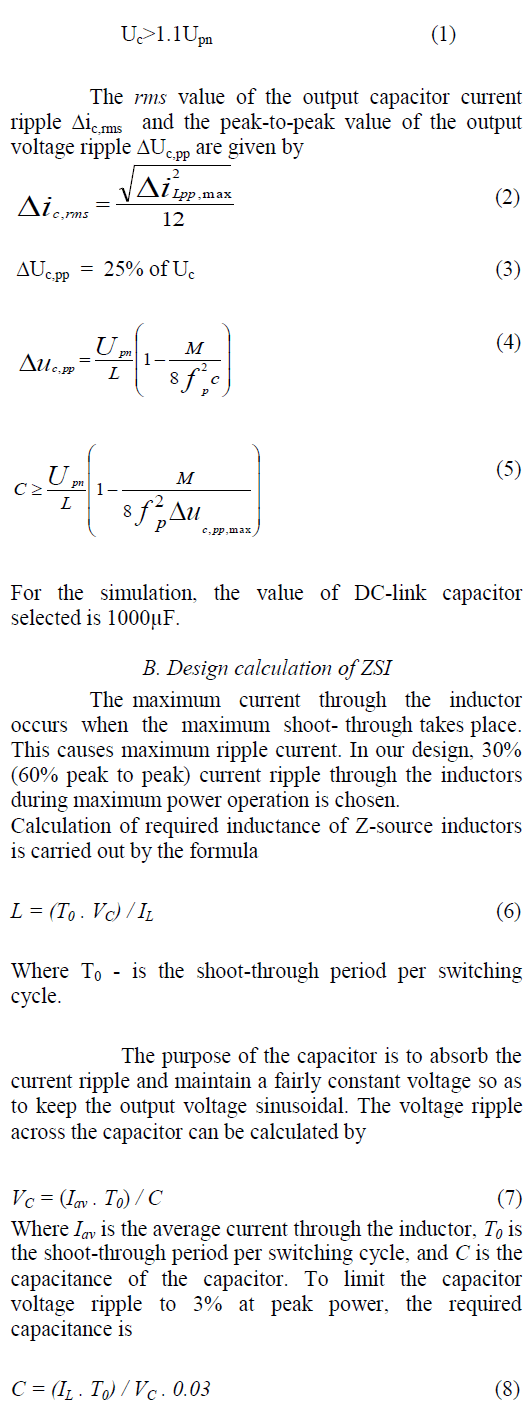
| The SR is a buck type AC to DC converter. The output of SR is obtained across the DC-link capacitor which is used for filter out the AC components present at the output of the rectifier. When selecting the output capacitor C, the value of the controlled output voltage Upn and an additional overshoot margin to enable safe operation during load transients (around 10% of Upn), must be taken into consideration. |
 |
| The values of the inductor and the capacitor are greatly dependent upon the rating of the motor, whose speed is to be regulated. Therefore the motor ratings are, 3-phase induction motor, star connected. Power 0.75KW, Speed - 1390 rpm Voltage - 415V, Current - 1.80 A Frequency - 50Hz, Efficiency - 75%. |
| For the overall circuit simulation and hardware construction the values of the capacitor and inductor used are 1000μF and 6.8mH respectively. |
III. SIMULATION DIAGRAM OF ASD WITH SR AND ZS I |
| The SR is buck type AC to DC converter which consist of diode bridge along with main switches T+ and T- and current injection network Sy1, Sy2, Sy3. The ZSI consists of voltage source from the DC supply, Impedance network, and three phase inverter and with AC motor load. AC voltage is rectified to DC voltage by the SR. This rectified output DC voltage fed to the Impedance source network which consists of two equal inductors (L1, L2) and two equal capacitors (C1, C2).The network inductors are connected in series arms and capacitors are connected in diagonal arms. The impedance network is used to buck or boost the input voltage depends upon the boosting factor. This network also act as a second order filter At normal condition the input voltage is 230 V. At the time of voltage sag the input supply is 50 V which can be implemented to the system using two controlled switches. The simulation diagram is shown in Figure1. |
 |
IV. EXPERIMENTAL RESULTS |
| The DC-link voltage and current and speed of the IM are compared for conventional system (Drive using diode bridge rectifier and voltage source inverter) and proposed model (Drive using SWISS rectifier and Zsource Inverter). |
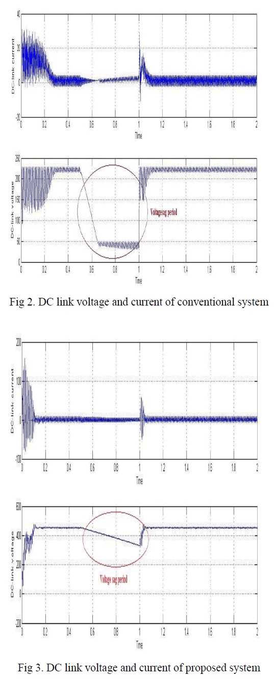 |
| The waveforms of DC-link voltage and current of conventional and proposed systems are shown in Figure 2 and Figure 3 respectively. In conventional method voltage at normal condition is 230V. When fault occur (ie, between 0.5 S to 1S) voltage decreased to sag voltage ie, 50 V. In the proposed model voltage at normal period is 450 V and at sag condition there is a decrease in voltage ie, voltage is decreasing from 450V to 330V,but this voltage is sufficient to drive the IM. This DC link voltage is given to the ZSI. |
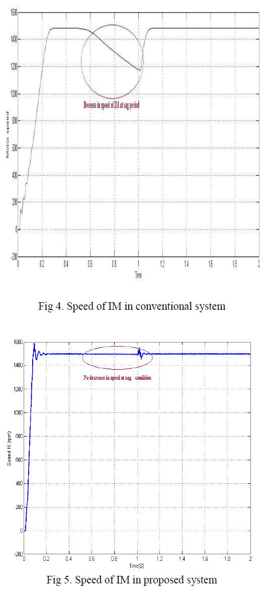 |
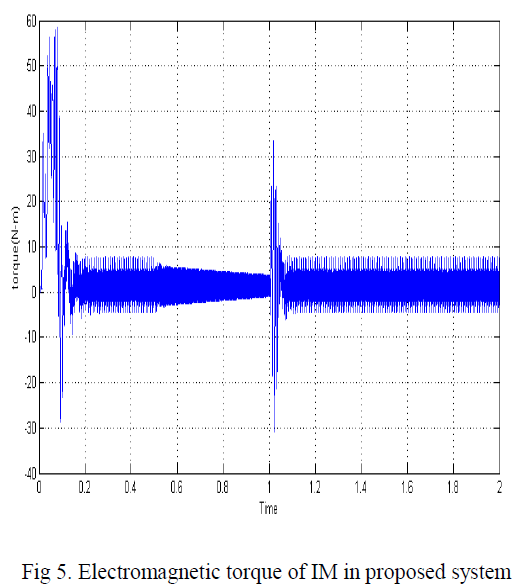
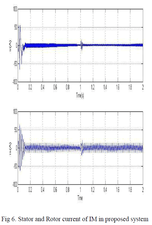
| The speed of IM for conventional and proposed system are shown in Figure 4 and Figure 5 respectively.In conventional method the decrease in DC-link voltage is not sufficient to drive the IM and there is decrease in speed.But in the proposed model there is no decrese in speed at the sag condition.ie, the proposed model ie,the ASD using SWISS rectifier and Z-source inverter is capable of mitigating the voltage sag at the time of fault and the drive can operate effectively. The electromagnetic torque and the current through stator and rotor of IM for the proposed system is shown in Figure 5 and Figure 6 respectively.The analysis of the waveform and the comparison with the existing model is given in Table 1. |
 |
 |
 |
V. CONCLUSIONS |
| Voltage sag mitigation can be done effectively in ASD using SR at the front side and ZSI at the back end side. The simulations were done for both proposed system and conventional systems and a comparative study is done for both system. |
| In conventional method there is a sudden decrease in voltage at the DC link at the time of fault and this voltage is insufficient to drive the IM. In the drive using SR and ZSI, the SR provide more controlled voltage and is given to the ZSI. The ZSI is a buck boost inverter which provide both buck and boost operation. The controlled voltage at the DC link is sufficient to drive the IM even in the fault condition. So drive can operate effectively at the time of voltage sag. |
ACKNOW LEDGMENT |
| would like like to thank the head of the department and colleagues of the rajalakshmi engineering college for encouraging and supporting for me to do this work. |
References |
|