Keywords
|
| Asynchronous data sampling, DETFF, clock-gating. C-element, delay buffer, ring-counter |
INTRODUCTION
|
| Portable multimedia and communication devices have experienced explosive growth recently. longer battery life is one of the crucial factors in the widespread success of these products. as such, low-power circuit design for multimedia and wireless communication applications has become very important. in many such products, delay buffer make up a significant portion of their circuits. For a sequential system, the power spent on the clocktree or the timing components is a major source of all the power consumption. The clock system, which consists of the clock distribution network and timing elements is one of the most power consuming components in a VLSI system. It consumes for 30% to 60% of the total power dissipation in a system. As a result, reducing the power consumed by flip-flops will have a deep impact on the total power consumed. In modern integrated circuits(ICs) the power consumed by two ways. |
| One effective and efficient approach is Double edge triggered flip flop (DETFF). Dual edge clock triggering requires Dual Edge- Triggered Storage Elements (DETSE), capable of capturing data on both rising and falling edge of the clock[4]. Main advantage of DETSE is their operation at half the frequency of the conventional single-edge clocking, while obtaining the same data throughput. |
| In addition to gating the clock signal going to the DET flip-flops[2] in the ring counter, and also proposed to gate the drivers in the clock tree. The technique will extremely decrease the loading on distribution network of the clock signal for the ring counter and thus the overall power consumption. The same technique is applied to the input driver and output driver of the memory part in the delay buffer. The rest of the paper organizes as follows: Section II describes the general concept of asynchronous data sampling and the next section explains the delay buffer with gated ring counter and driver tree concepts. The third Section describes the simulation results and finally Section IV |
ASYNCHRONOUS DATA SAMPLING
|
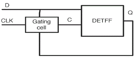
| The clock gated system has the terminology as global clock CLK ; the (internal) gated clock signal C;, clock-gating control signal CG; , input data D; and , output data Q. the internal clock controls the gated circuits. The internal clock is separated from the global clock. If the internal clock is not synchronize with the global clock when the gating signal is in non-active state, then the internal clock need to switch immediately to match the global clock. This switching is extra and not synchronized with the external clock, which creates an asynchronous data sampling, which is cleared by the output changes between two clock edges. |
| Each clock-gating transition has the potential to create the asynchronous sampling issue. The specific conditions deals with the creation of asynchronous data sampling with clock gated double edge triggered flip flop is given below. |
DELAY BUFFER
|
| SRAM-based delay buffers are more popular in long delay buffers because of the compact SRAM cell size and small total area. Also, the power consumption is much less than shift registers because only two words are accessed in each clock cycle: one for write-in and the other for read-out. A binary counter can be used for address generation since the memory words are accessed sequentially. In the proposed delay buffer, several power reduction techniques are adopted. Mainly, these circuit techniques are designed with a view to decreasing the loading on high fan-out nets, e.g., clock and read/write ports. |
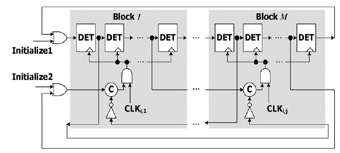
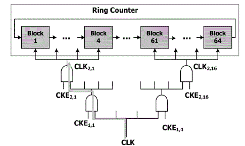
| A. GATED-CLOCK RING COUNTERC-element and to use tree-structured clock drivers with gating so as to greatly reduce the loading on active clock drivers. Additionally, DET flip-flops are used to reduce the clock rate to half and thus also reduce the power consumption on the clock signal. |
| B. GATED-DRIVER TREE |
| Driving the input signal all the way to all memory cells seems to be a waste of power. The same can be said for the read circuitry of the output port. In light of the previous gated-clock tree technique, we shall apply the same idea to the input driving/output sensing circuitry in the memory module of the delay buffer. |
| The memory words are also grouped into blocks. Each memory block associates with one DET flip-flop block in the proposed ring counter and one DET flip-flop output addresses a corresponding memory word for readout and at the same time addresses the word that was read one-clock earlier for write-in. |
| C. TECHNIQUE USED TO AVOID SAMPLING PROBLEM |
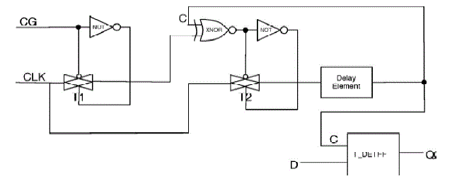
| This section describes how the sampling problem addressed and removed. generally Sampling problem shares the same root cause, namely the discontinuity between the global and internal clock. If the internal clock differs from the global clock when clock gating is discontinued, then the internal clock event is transmitted immediately.The CLK is controlled by the comparison D of Q and . If D has changed since the last clock transition and is different from Q , then CLK will pass to the second comparator to compare with the C . This CLK & C comparator controls the switch T2 between C the and CLK. This second comparator prevents the asynchronous sampling occurs in this implementation. Asynchronous sampling occurs when D changes at the moment that CLK differs from.However, with the second CLK &C comparator in Figure 4 , the switch T2 will stay OFF when CLK≠C , and C will synchronize with CLK. In the next half cycle where CLK = C , the switch T2 turns ON, but since they are equal, the flip-flop will not be triggered until C changes, which follows CLK when T2 is ON. The delay element in the proposed clock gating circuit-1 is created a Δ??, the time difference between the CLK edge and comparator output signal, which allows C to change and then trigger the flipflop. |
SIMULATION RESULT AND DISCUSSIONS
|
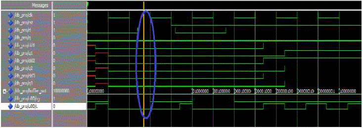
| The simulation result describes gated clock ring counter without sampling problem by implementing the gated double edge triggered flipflop. Here the c-element activate the counter for every clock pulse. |
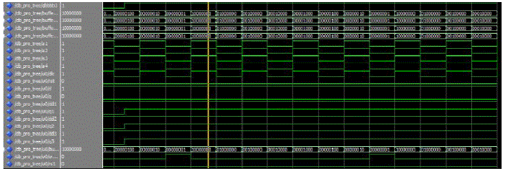
| The above shown simulation results describes the gated driver tree without sampling problem. It was designed with multiple ring counter forming as a tree structure. The output of the first block (which contains the ring counter with four flipflops) is given to the second block same as the previous. |
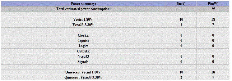
| The simulation result of gated clock ring counter with removal of asynchronous behavior of the internal clock signal, clock gating technique which is used to avoid asynchronous behavior of the Internal Clock Signal by the condition of CLK ≠C.CLK is controlled by the comparison of D and Q If D has changed since the last clock transition and is different from Q, then CLK will pass to the second comparator to compare with the C . This CLK&C comparator controls the switch T2 between the C and CLK. The above figure shows the power consumption is about 25mw. The simulation result shows the power consumption about 24mw which is consumed by the clock driver tree. |
| The table.2 describes the power consumption and gate count(area) occupied by the gated clock ring counter as 25 mw and 120 gates and the gated driver tree as 24mw and 748 gates without asynchronous data sampling. |
CONCULSION
|
| The low power delay buffer circuit has been proposed and designed, based on the dual edge triggered structure. And also the gated driver tree designed by using the delay buffer which is adopted by ring counter strategy. To reduce the dynamic power consumption, a number of low-power techniques such as clock gated (celement) is implemented at the system level. DETFF achieves substantial power reduction by incorporating dual edge triggering and clock gating. However, when applying clock gating into a DETFF, a data transition error may appear at the output between clock edges due to asynchronous data sampling in the gated clock ring counter. All gating signals are easily generated by a C-element taking inputs from some DET flip-flop outputs of the ring counter. The special gating technique is proposed for sampling problem and results are discussed with consumed power and area. |
ACKNOWLEDGMENTS
|
| We thankful to our Head of the Department, Prof. Mr. Muthukrishnan for his guidance and help. We express our heartiest gratitude for our project guide Asst Prof. Mr.S.UdhayaKumar for his everlasting support and help. He gave shape to our abstract idea and made everything possible. His timely guidance is the reason for the systematic completion of the project. |
Tables at a glance
|
 |
 |
| Table 1 |
Table 2 |
|
| |
Figures at a glance
|
 |
 |
 |
 |
| Figure 1 |
Figure 2 |
Figure 3 |
Figure 4 |
 |
 |
 |
 |
| Figure 5 |
Figure 6 |
Figure 7 |
Figure 8 |
|
| |
References
|
- A. G. M. Strollo, E. Napoli, and D. De Caro,2003june “New clock-gating techniques for low power flip-flops,” in Proc. Int. SympLow Power Electronics and Design.
- C.-C. Yu, 2008, “Low-power double edge-triggered flip-flop circuit design,” in Proc. Int. Conf. Innovative Computing Informationand Control , pp. 114–119.
- H. Karimiyan, S. M. Sayedi, and H. Saidi, 2010 “Low-power dual-edge triggered state retention scan flip-flop,” IET Comput. & Dig.Techniques, vol. 4, no. 5, pp. 410 ,419.
- N. Nedovic and V. G. Oklobdzija, Oct. 2005 ,“Dual-edge triggered storage elements and clocking strategy for low-power systems,”IEEE Trans. Very Large Scale Integration (VLSI) Syst., vol. 13, no. 5, pp. 577–590,.
- P. Zhao, J. McNeely, P. Golconda, M. A. Bayoumi, R. A. Barcenas, and W. K.W Kuang, Jun. 2007 “Low-power clock branch sharingdouble-edge triggered flip- flop,” IEEE Trans. Very Large Scale Integ. (VLSI) Syst.,vol. 15, no. 3.
- Q. Wu, M. Pedram, and X. Wu, Mar. 2000 “Clock-gating and its application to low power design of sequential circuits,” IEEE Trans.Circuits Syst. I: Fundam. Theory Appl vol. 47, no. 3, pp. 415–420,.
- W.-S. Tam, S.-L. Siu, C.-W. Kok, and H. Wong, 2010,“Double edge-triggered half- static clock-gated D-type flip-flop,” in Proc. IEEEInt. Conf. Electron Devices Solid- State Circuits (EDSSC), pp. 1–4.
- X. Wang and W. H. Robinson, 2010 “A low-power double edge-triggered flip-flop with transmission gates and clock gating,” in Proc.IEEE Int. Midwest Circuits and Systems (MWSCAS), pp. 205–208.
- G. Pastuszak, “A high-performance architecture for embedded block coding in JPEG 2000,” IEEE Trans. Circuits Syst. VideoTechnol., vol.15, no. 9, pp. 1182–1191.
- Q. Wu, M. Pedram, and X. Wu, Mar. 2000 “Clock-gating and its application to low power design of sequential circuits,” IEEETrans. Circuits Syst. I: Fundam.TheoryAppl vol. 47, no. 3, pp. 415–420.
|