ISSN ONLINE(2319-8753)PRINT(2347-6710)
ISSN ONLINE(2319-8753)PRINT(2347-6710)
Mahendra.B.M1, Ramachandra.A.C2
|
| Related article at Pubmed, Scholar Google |
Visit for more related articles at International Journal of Innovative Research in Science, Engineering and Technology
The complications of System-on-a-Chip (SoC) functional verification have become more and more complexity. To improving verification productivity and avoiding respins have led to a structured, design-for-verification methodology. In the past decades, many functional verification tools and methodologies have been developed, including simulators, formal verification and debugging tools. Constraints Random Verification (CRV) combines automatic test generation, self-checking test benches, and coverage metrics to significantly reduce the time spent on verifying a design and ensuring throughput of verification by developing Verification Intellectual Property (VIP) for different on-chip interconnect Intellectual Property (IP) blocks on SoCs. The proposed Methodology of Coverage Driven Constraint Random Verification is validated using illustrative example of Advanced microcontroller bus architecture (AMBA) advanced extensible interface (AXI) Protocol for on-chip bus infrastructure where in development design process involves 35% of Designers interference and 65% of Verification Interference. This paper provides a unique approach for successful completion of design and verification with reduced development design cycle.
Keywords |
| System-on-chip (SoC), Intellectual Property (IP), AMBA, AXI, VIP, CRV, CDV |
INTRODUCTION |
| As semiconductor technology improves, System-On- Chip (SoC) designs are becoming popular. A SoC platform usually consists of various design components dedicated to specified application domains. In order to ensure the functional correctness of a SoC, finding and fixing the design errors at early design phases is important in today’s hardware development flows. The process of finding design errors is called “verification”. However, as design complexity increases, experience shows that many bugs remain undetected even though considerable resources and time have been devoted to design verification, which can cause serious problems. |
| Due to the importance of ensuring a design’s functional correctness, a great deal of effort has been devoted to design verification in order to reduce verification effort and promote design quality. However, most existing direct test simulation-based verification techniques cannot guarantee sufficient coverage of the design, resulting in undetected bugs. Furthermore, they cannot accurately handle non-deterministic problems that are becoming more and more important nowadays. In order to overcome the limitation of direct test verification & random verification techniques, constraint random verification (CRV) to verify design correctness has been proposed as a promising alternative to direct test simulation. To improve design quality and reduce verification effort, we propose Coverage Driven Constraint Random Verification in this dissertation. |
| With advances in semiconductor technology, functional verification continues to remain one of the primary challenges in SoC designs today. As the statistics in industry surveys show, despite the fact that up to 70% of project resources have been devoted to functional verification, only 33% of SoC designs are correct on the first pass, and 75% of all design flaws are attributable to logic or functional bugs due to shortcomings in functional verification. |
| Improving verification productivity and avoiding respins have lead to a structured, design-for-verification methodology. In the past decades, many functional verification tools and methodologies have been developed. Among these verification methods, Constrained-Random Verification (CRV) has become the mainstream methodology for functional verification to generate as large a representative set of scenarios for a given protocol as possible under project constraints. However, it is shown that CRV methods can’t provide the reliability assurance required. One of the specific challenges people are having today is using constrained random simulation methods to reach coverage goals. The Coverage Driven Verification (CDV) combines automatic test generation, self -checking, testbenches, and coverage metrics to significantly reduce the time spent verifying a design and reach the coverage goal. It track progress with functional coverage to ensure test plan criteria are met and also ensure corner cases are hit. System Verilog language provides additional flexibility for writing constraints. This method contributes to the overall verification methodology by ensuring well-defined properties that can guarantee the correctness in and between blocks. This improves modularity of verification and enables finding bugs in the design process when they are easier to understand and fix. |
AMBA FAMILY AND AXI PROTOCOL BACKGROUND |
| AMBA was introduced by ARM Ltd in 1996. The first AMBA buses were Advanced System Bus (ASB) and Advanced Peripheral Bus (APB). In its 2nd version, AMBA 2, ARM added AMBA High-performance Bus (AHB) that is a single clock-edge protocol. In 2003, ARM introduced the 3rd generation, AMBA 3, including AXI to reach even higher performance inter-connects and the Advanced Trace Bus (ATB) as part of the Core-Sight onchip debug and trace solution. In 2010 the AMBA 4 specifications were introduced starting with AMBA 4 AXI4, then in 2011[4] extending system wide coherency with AMBA 4 ACE. In 2013 the AMBA 5 CHI (Coherent Hub Interface) specification was introduced, with a redesigned high-speed transport layer and features designed to reduce congestion. |
| We will go through in details overview of AMBA AXI4 architecture [3] which supports data transfers up to 256 beats and unaligned data transfers using byte strobes. In AMBA AXI4 system 16 masters and 16 slaves are interfaced. Each master and slave has their own 4 bit ID tags. AMBA AXI4 system consists of master, slave and bus (arbiters and decoders). The system consists of five channels namely write address channel, write data channel, read data channel, read address channel, and write response channel. The silent Feature of AXI4 protocol: |
| Separate address/control and data phases |
| Separate address/control and data phases strobes |
| Burst-based transactions with only start address issued and Variable-length bursts from 1 to 16 data transfers per burst. |
| A burst with a transfer size of 8, 16, 32, 64, 128, 256, 512 or 1024 bits wide is supported. |
| Updated AWCACHE and ARCACHE signalling details. |
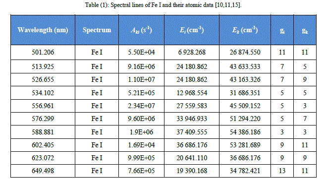
| Each transaction is burst-based which has address and control information on the address channel that describes the nature of the data to be transferred. The data is transferred between master and slave using a write data channel to the slave or a read data channel to the master. Table 1 gives the information of signals used in the complete design of the protocol. The write operation process starts when the master sends an address and control information on the write address channel as shown in figure1. The master then sends each item of write data over the write data channel. The master keeps the VALID signal LOW until the write data is available. The master sends the last data item, the WLAST signal goes HIGH. When the slave has accepted all the data items, it drives a write response signal BRESP [1:0] back to the master to indicate that the write transaction is complete. This signal indicates the status of the write transaction. The allowable responses are OKAY, EXOKAY, SLVERR, and DECERR. After the read address appears on the address bus, the data transfer occurs on the read data channel as shown in figure 2. The slave keeps the VALID signal LOW until the read data is available. For the final data transfer of the burst, the slave asserts the RLAST signal to show that the last data item is being transferred. The RRESP[1:0] signal indicates the status of the read transfer. The allowable responses are OKAY, EXOKAY, SLVERR, and DECERR. |
 |
RELATED WORK |
| In order to reduce the risk and pressures of a new design is through the use of standards and reuse. Today, designers can also choose from a range of open specifications of on-chip interface protocols. Choosing this option facilitates use of proven, predesigned, preverified IP and verification components. With more proven IP in the design and by the deployment of Verification IP (VIP), designers can focus on differentiating their design rather than verification of the standard based protocol. |
| Many CAD tool development companies provide different flavours of verification IP for existing standard protocol IP like CORE CONNECT [5] developed by IBM, WISHBONE developed by Silicore Corporation [6] and AMBA [4] developed by ARM. Example Synopsys Discovery VIP for AMBA,USB, etc., provide a protocol-centric debug environment with built verification plans and coverage points to achieved design development process and even To verify on-chip communication properties rule based synthesizable AMBA AXI protocol checker [2] is used. |
PROPOSED WORK |
| This dramatically reduces the overall risk associated with the design. Deployment of a layered verification methodology combined with the use of constrained random verification techniques are required to meet the challenge of verifying a subsystem which uses the AMBA AXI protocol. As discussed earlier, a directed testing methodology cannot create enough system stimuli to reach the required coverage goals in the shortened design cycle. In this project the AXI master VIP has been developed to verify AXI slave for convenient let’s consider the slave as memory model on which Development of a layered verification methodology combined with the use of constrained random verification techniques is used. |
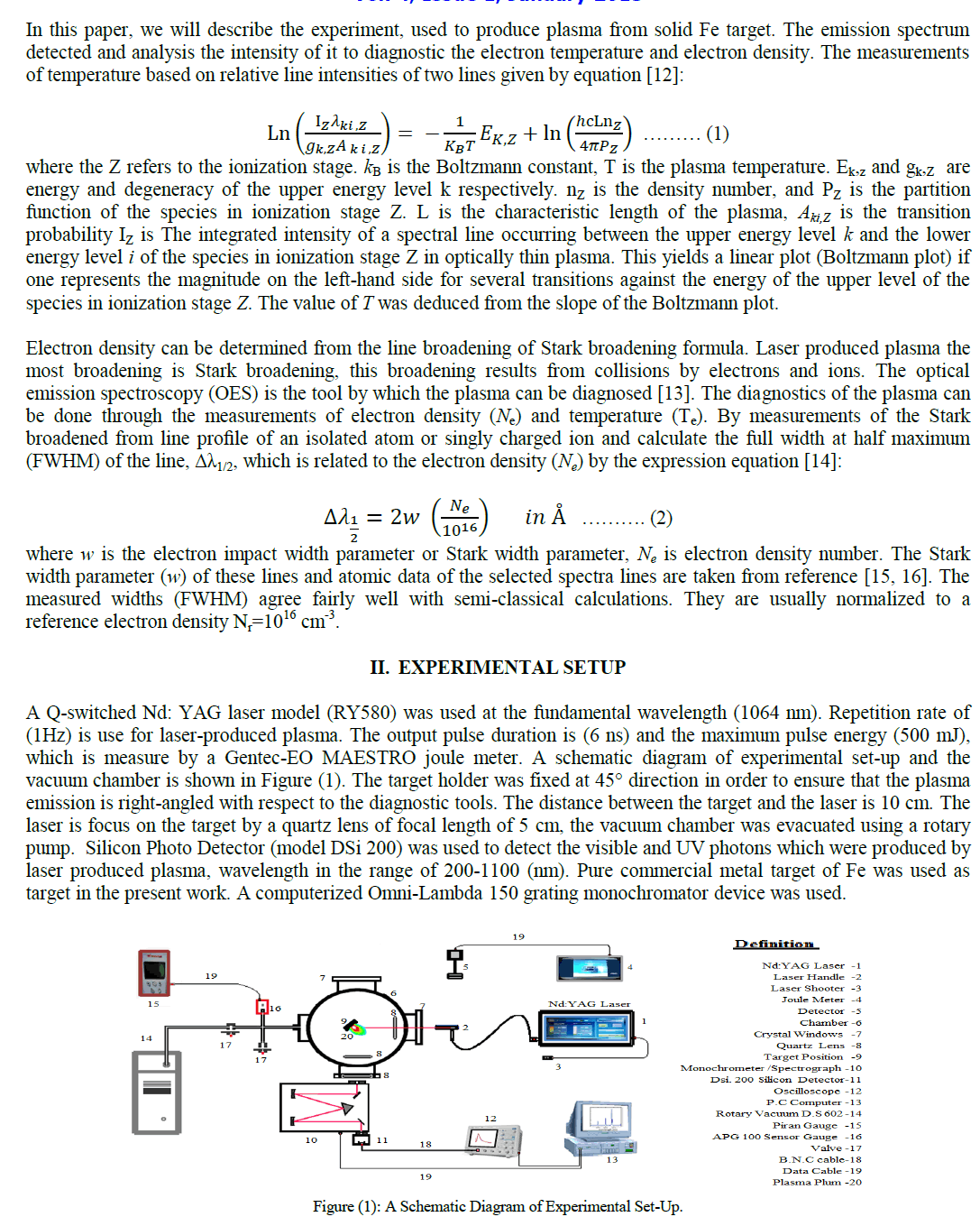 |
| The AXI protocol provides a single interface definition for describing interfaces |
| between a master and the interconnect |
| between a slave and the interconnect |
| between a master and a slave. |
| In this technique with a layered verification approach, lower layers like protocol verification are reused at higher levels. Tests written for the lowest levels, protocol validation are reused at the higher levels where the verification focus shifts to generating and verifying transaction sequences that not only stress the bus interface logic but can also target the application specific logic. |
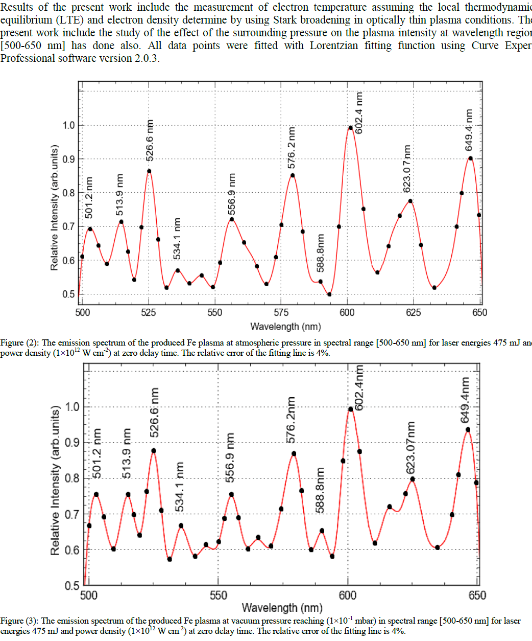 |
| In the layered based constraint random verification environment consist of following components |
| a. Test: which interact with all the layers and allows passing directed commands to functional and command layer. |
| b. Scenario: which produce sequences of transactions that are applied to the functional layer that has set of weights, constraints or scenarios specified by test layer. c. Functional: This contains higher-level driver and monitor components and even self-checker. d. Command: This layer contains lower-level driver and monitor components, as well as the assertions. |
| e. Signal: This layer connects the Test bench to the DUT. It consists of interface, clocking, and modport constructs. |
SIMULATION RESULTS |
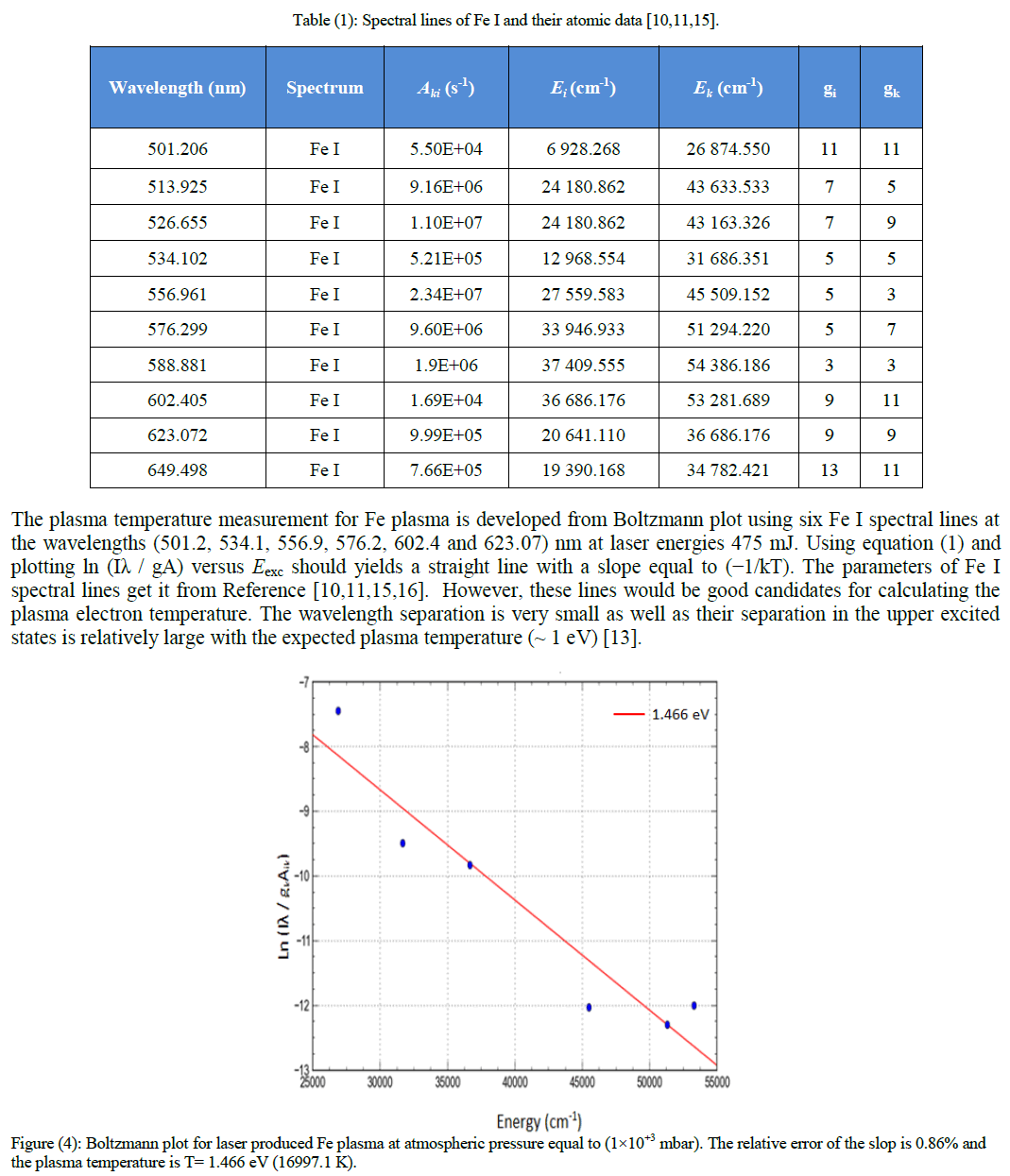
| Simulation is being carried out on QuestaSim [9] which is trademark of Mentor graphics, using System Verilog [10] as hardware verification language. The test cases are run for multiple operations and the simulation log file and coverage reports are analyzed. The main advantage of systemverilog is reusabilty of verification code for different test scenarios and also interconnect to different AXI slave IP block. The different test case patterns are used to verify the AXI slave. The AResetn signal is active low. Master drives the address, and the slave accepts it one cycle later. The write address values passed to module as 72 with incremental burst of 16 as shown in figure 3 and the simulated results for burst read operation with start address as zero with incremental burst of 16 as shown in figure 4. |
 |
 |
CONCLUSIONS |
| This work helps to understand the complete functional verification process of complex ASICs an SoC’s and it gives opportunity to try the latest verification methodologies, programming concepts like Object Oriented Programming of Hardware Verification Languages and sophisticated EDA tools, for the high quality verification. |
| The functionality of AXI slave IP is verified using CDV and observed the code coverage & functional coverage using coverpoints and cross coverpoints. The CDV methodology can be used to make reusable test benches successfully. The result shows that 99.96% of functionality is covered and average code coverage of 91.56% {with statement coverage of 95%, Branch coverage of 100% and toggle coverage of 90.45%} |
ACKNOWLEDGMENT |
| The authors would like to thank Vlsiguru training institute for providing access to Questasim EDA tool and technical supports. |
References |
|