ISSN ONLINE(2319-8753)PRINT(2347-6710)
ISSN ONLINE(2319-8753)PRINT(2347-6710)
Nayana. A1, Prof.A.Mala2
|
| Related article at Pubmed, Scholar Google |
Visit for more related articles at International Journal of Innovative Research in Science, Engineering and Technology
A single-inductor dual-output (SIDO) buck converter has recently found applications in hand-held battery-powered electronic devices. The circuit operation and the functional interdependencies among basic converter parameters such as dc voltage gains, transistor duty cycles, and load current levels are much more complicated than those of the single-output counterpart. In this paper, a rigorous analysis was conducted to develop dc equations in steady state operation for SIDO converters. More importantly, from the analysis results, a possibility of a new mode of operation, dubbed “mix-voltage” operation, will be pointed out. In the so-called “mix-voltage” operation, the converter is capable of working even when the input voltage is lower than one of the two output voltages. In the past, a SIDO buck converter has been used for providing “pure-buck” outputs, i.e., both output voltages are lower than the input voltage. Therefore, this possibility not only opens up new applications but also extends the operating battery range in existing applications .Simulation results confirmed the dc equations and the “mix-voltage” conversion of SIDO buck converters. The closed loop analysis of SIDO converter in mixvoltage conversion using PI and Fuzzy .controllers against load variations is analyzed. Based on the analysis, performance of the converter using both controllers is compared. Simulation results are presented to validate the proposed converter topology.
Keywords |
| DC–DC power converters, mix-voltage conversion, single-inductor dual-output (SIDO). |
INTRODUCTION |
| A SINGLE-inductor dual-output (SIDO) buck converter has recently found applications in hand-held batterypowered electronic devices, which require dual outputs but no electrical isolation [1]–[3]. The main attraction of a SIDO lies in the fact that dual regulated outputs can be provided with relatively low cost and small size. The circuit diagram of SIDO Buck converter may look simple but the circuit operation and the functional interdependencies among basic converter parameters such as dc voltage gains, transistor duty cycles, and load current levels are much more complicated than the counterparts of a conventional single-output buck converter. |
| In this paper, a rigorous analysis in steady-state operation would be conducted to develop useful equations for design purposes. More importantly, from the analysis results, a possibility of a new mode of operation, dubbed “mixvoltage” operation would be pointed out. In the so-called “mix-voltage” operation, the input voltage can be lower than one of the output voltages, as opposed to conventional “pure-buck” operation in which input voltage must be higher than both output voltages. This implies that the input battery may operate down to a voltage level lower than previously thought possible. This may also mean that a single battery, instead of two in series, is sufficient in some applications. |
| In case of load variations, output voltage of a power supply is not regulated .In order to regulate the output voltage and predict the performance of the device against load variations, closed loop analysis of the converter is necessary. Hence the closed loop analysis of the SIDO converter using PI and Fuzzy controller is done and the performance of the device is compared. |
 |
| The paper has been organized as follows: Chapter II gives a basic review of SIDO buck converter. Analytical equations relevant to continuous and discontinuous conduction mode, dc voltage gains, and duty cycles will be developed for both the “pure-buck” and the “mix voltage” operations. It also describes an algorithm for determining the SIDO Buck-operating mode and duty cycle values .Chapter III describes mix voltage conversion and also derives an equation to estimate the mix-voltage conversion minimum operable input voltage. Since a SIDO buck converter is mostly used in low voltage applications, semiconductor switch conduction voltage drops will be included in the analysis for accuracy. Chapter IV describes the closed loop analysis of the SIDO buck converter using PI and Fuzzy controllers. Chapter V explains the MATLAB simulation of SIDO buck converter using the controllers. Chapter VI gives results of simulation and the performance comparison of the device using both the controllers. Finally, conclusions of this work are summarized in Chapter VII. |
OPERATION OF SIDO BUCK CONVERTER |
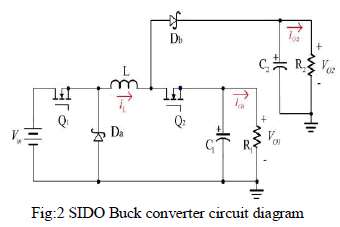
| The power circuit diagram of a SIDO buck converter is shown in fig:2 |
 |
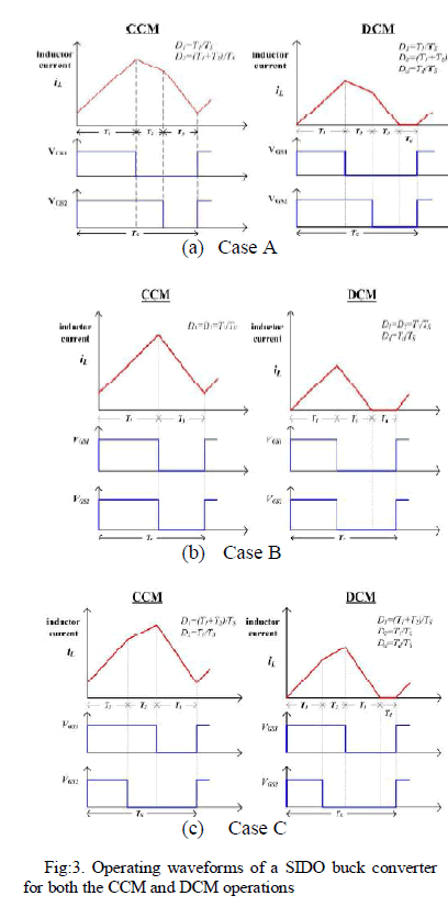
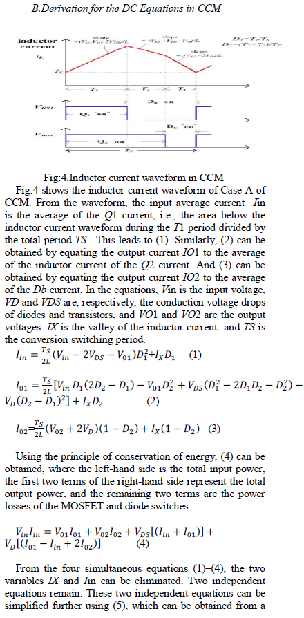
| A SIDO buck converter can be operated in both the continuous conduction mode (CCM) [2], [5]–[10] and discontinuous conduction mode (DCM) [11], [12], just like a conventional single-output buck converter. Fig. 2 shows the waveforms of the inductor current and transistor duty cycles with a time multiplexing control scheme [13] for both the CCM and DCM operations. According to the relative magnitude of transistor Q1 duty cycle D1 and transistor Q2 duty cycle D2, the waveforms are given for three cases: Case A (D1 < D2 ), Case B (D1 = D2 ), and Case C (D1 > D2 ). In the CCM operation, there are three periods: T1 is the duration when both transistors Q1 and Q2 are ON. During this period, diodes Da and Db are OFF and the power is provided to VO1 only. The period T2 is the period when only one of the transistors is in conduction. If Q1 , instead of Q2 , is in conduction, then the inductor current flows through Db and the power is provided to VO2 only. Otherwise, it flows through Da and the power is provided to VO1 only. The period T3 is the period when both transistors are OFF. The inductor current is then flowing through Da and Db , and the power is provided only to VO2 . Notice that D1 is, therefore, equal to T1/TS or (T1 + T2 )/TS , where TS is the conversion switching period, depending upon whether it is Case A, B, or C. The same situation applies to D2 . It is also clear that there is no T2 period for Case B. All of these are shown along with the waveforms in Fig. 2. For the DCM operation, there is an additional period Td when the inductor current stays at zero and none of the switches is on. The duty cycle Dd is defined as Td/TS . |
 |
 |
 |
| D. Algorithm for Determining the SIDO Buck-Operating Mode and Duty Cycle Values |
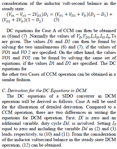
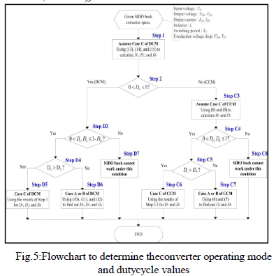
| Normally, converter component values and operating conditions are given. From the equations in Tables II and III, one can see that if duty cycles D1 , D2 , and Dd are known, then proper Case and, therefore, proper equations can be selected to solve for the output voltages VO1 and VO2 . However, it is more difficult to do that the other way around, that is, to determine the duty cycle values from the specified output voltage values. This is because, to use the proper equations, one needs to know in advance in which mode (CCM or DCM) and in which Case (A, B, or C) the converter is being operated. This information can only be found out with an elaborate procedureHence an algorithm is proposed to do that which is shown in fig.5 |
| In the top block, a set of values including output voltages, component values, switching period, and input voltage are given. In Step 1, one assumes that the converter operates in Case C of DCM, and therefore, uses the corresponding equations to find out the values D1 , D2 , and Dd. In Step 2, Dd is used to determine the converter operation mode. If Dd is within the range of [0, 1], then it is a DCM operation. If not, then it is a CCM operation. In Step D3, the duty cycle D1 and D2 values are checked to see if they stay in proper boundary. Obviously, they cannot be a complex number and have to be within the range of [0, 1-Dd ]. If not, then there is no answer to the given set of starting parameters. In other words, it is not possible for a SIDO converter to provide the specified VO1 and VO2 under the specified conditions and parameters as indicated by Step D7. If otherwise, go to Step D4. In Step D4, it must be checked if D1 > D2 (Case C) because it was initially assumed to be Case C in Step 1. If the answer is “yes”, then the values D1 , D2 and Dd obtained in Step 1 are the final answers.Otherwise, go to Step D6 and use Case A or B equations tofind out the duty cycle values. The discussion that took place earlier applies to the situation if the decision in Step 2 is “yes”. If the decision in Step 2 is “no”, then go through the CCMpath to Step C3 and first assume it is in Case C and solve for the duty cycles. The rest of the path follows the same logic as used in the DCM path. At the end, either an answer can be found or it is not possible to meet the beginning specifications of the SIDO converter. This flowchart will be used in the next section to illustrate the “mix-voltage” conversion. |
MIX-VOLTAGE CONVERSION FOR SIDO BUCK CONVERTER |
| Mix-voltage conversion mode is a new mode of operation proposed in SIDO buck converter.In this mode of operation the converter is capable of operating even when the input voltage is lower than one of the two output voltages. In the past, a SIDO buck converter has been used for providing “pure-buck” outputs, i.e., both output voltages are lower than the input voltage. But in Mix-Voltage it is proved that the converter can give both buck and boost outputs. . It means that input can be lower than any one of the output voltages.There is a minimum operable input voltage up to which mix- voltage”conversion is possible. Mix voltage conversion can be explained with the help of the previously described flowchart.. |
| Example 1: Converter specifications are given in the following. |
| VO1 = 1.8V, VO2 = 3.3V, IO1 = 500mA, IO2 = 200mA, L = 10 μH, VDS = 0.01 V, VD = 0.4 V, and TS = 5 μs. The maximum input voltage Vin max = 5 V. Find the duty cycle information and the minimum operable input voltage Vin min. |
| Step 1: Vin is first set at 5 V and proceeded as follows: Two sets of solutions are obtained using (13)–(15). |
| (D1,D2,Dd) ={(−0.6763,−0.7931, 2.255) and (0.6763, 0.7931, −0.2546)} |
 |
| Step 2: Since Dd is outside the range of [0, 1] for both solutions, the converter works in CCM; therefore, go toStep C3. |
| Step C3: One set of solution is obtained (D1,D2) = (0.5335,0.6478) using (8) and (9). |
| Step C4: D1 and D2 stay within boundary. |
| Step C5: Need to check if D1 > D2 . It turns out D1 is less thanD2 . Thismeans the assumption in Step C3 and the equation used to obtain D1 and D2 were incorrect. Therefore, go to Step C7. The duty cycles need to be recalculated. |
| Step C7: Solving for D1 and D2 using (6) and (7). (D1,D2 ) = (0.5268, 0.6670). |
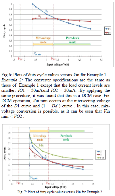
| The data given earlier were obtained for Vin = 5V. For each selected Vin value, the operating duty cycle values can be found as described earlier. It turns out that the converter operates in the CCM for the entire input range. Fig. 6 shows the plot of the resultant duty cycle values versus Vin. As Vin is decreased,the D1 curve intersects with the D1 = 1 line at Vin min. This crossover point is the minimum input voltage that the converter specifications can still be met by the converter because D1 must be no more than unity. From the figure, Vin min is about 2.36 V, which lies between VO1 and VO2 . This is mix-voltage conversion . This example shows that the converter is capable of operating even when the input battery voltage is well below VO2 value of 3.3 V. |
 |
| A Determination of the Minimum Operable Input Voltage |
| From the examples, one can find out the converter operating mode (CCM or DCM),the various duty cycle values, and the minimum operable input voltage Vin min. However, it would be much more convenient to the designers if Vin min can be calculated by an analytical expression. The following paragraph will discuss this issue. |
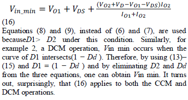
| For the first example in CCM operation Vin min occur when D1 is equal to unity. Therefore, by setting D1 = 1in (8) and (9) and eliminating D2 for the two equations, (16) can be obtained |
 |
CLOSED LOOP ANALYSIS OF SIDO BUCK CONVERTER |
| In a power supply ,the load variations are common load variations means sudden change of output current.In openloop,during load variations the output voltage of the converter is not regulated due to the effect of disturbances.Because of this issue closed loop analysis of the converter is proposed.In openloop,to get the regulated output voltage,we have to manually change the dutycycle of the switches.So the main purpose of closed loop control is to automatically control the dutycycle of the switches to regulate the output to a steady value with settling time, peak overshoot,integrated square error and steady state error as minimum. |
| The main purpose of closed loop control is to reduce the effect of disturbance on the output and to a maintain the output to a steady value.Inorder to maintain the output voltage to a regulated value, we have to automatically control the duty cycle of the switches. To automatically control the duty cycle of the switches, controllers are used. The output voltage of the converter is compared with reference voltage and error signal is produced. The error signal is given to the controller. The output of the controller is compared with a saw tooth signal and PWM signal is generated. These control signals are given as gating pulses for the switches. Hence the duty cycle of the switches is adjusted and output voltage can be regulated. In this project, PI controller and Fuzzy controllers are used for closed loop analysis. The comparative study of performance of the SIDO buck converter in mix-voltage conversion using both the controllers is done. |
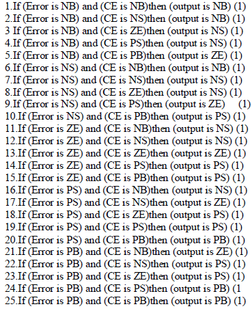
| In this paper, fuzzy controller is designed using the following rule base. The rule bases are developed based on the SLIDING RULE. |
 |
SIMULATION |
| In this section the matlab simulation of the proposed model is explained. |
| A.MATLAB/SIMULINK SIMULATION |
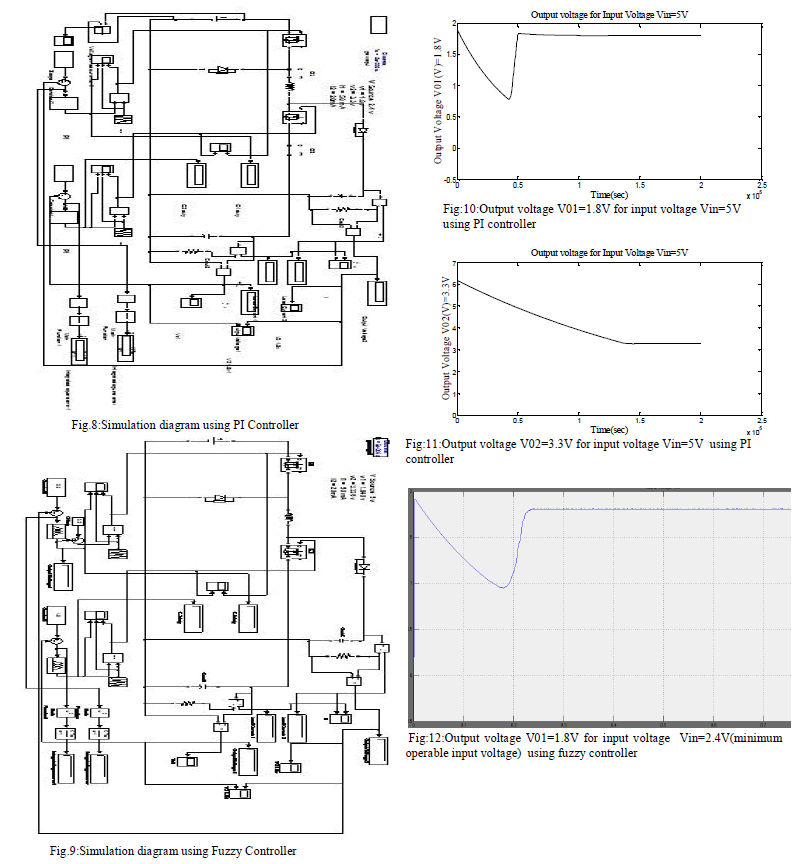
| The MATLAB/SIMULINK simulation diagram of the proposed system using PI &Fuzzy controller is shown in Fig.8 &9. |
| B.Comparitive Analysis |
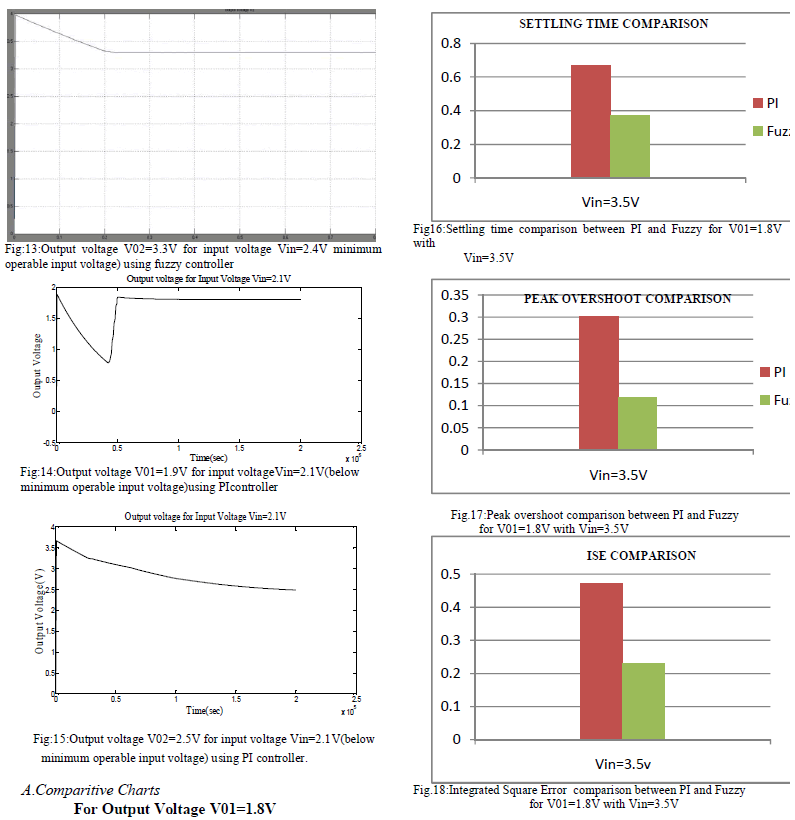
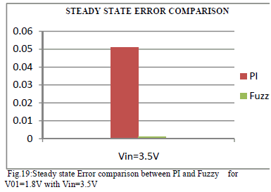
| Using Simulation ,the performance of SIDO buck converter in mixvoltage conversion using both the controllers are compared. The comparison parameters used are (i)Settling time( ts )in secs |
| (ii) Peak overshoot(Mp) in volt |
| (iii) Integrated square error |
| (iv) Steady state error. |
 |
 |
 |
 |
| From the simulation results the following conclusion can be obtained. |
| âÞâ Fuzzy controller requires very low settling time for output voltages compared to PI controller. |
| âÞâ Fuzzy controller causes low peak overshoot in output voltages compared to PI controller. |
| âÞâ The Integrated square error of output voltages is reduced using fuzzy controllers compared to PI controller. |
| âÞâ The Steady state error of output voltages is also reduced using fuzzy controllers compared to PI controller. |
| âÞâ The performance of SIDO buck converter with mix-voltage conversion using Fuzzy controller has good performance in output voltage against load variations compared to PI controller, almost shows the characteristics of an optimal controller. |
CONCLUSION |
| A SIDO buck converter was analyzed for steady-state operation.The various operating modes were explored and design equations were developed. These equationsallowthe designer to find out intricate relationships among output voltages, transistor duty cycles, and outputcurrents. From the results, a mix-voltage operation was pointed out and demonstrated. |
| The closed loop analysis of SIDO buck converter in mix- voltage conversion is analysed using PI and Fuzzy controllers. The performance of the converter using both controllers against load variations are analysed and discussed from simulation results.From the comparative analysis of the performance indices of the converter using both controllers in steady state, fuzzy controller shows better performance in steady state with settling time, peak overshoot, integrated square error and steady state error as minimum. The proposed method opens up new applications and may also extend the input battery operable range for existing applications.This proposed method can be implemented in hardware for future work. |
References |
|