International Journal of Advanced Research in Electrical, Electronics and Instrumentation Engineering
ISSN ONLINE(2278-8875) PRINT (2320-3765)
ISSN ONLINE(2278-8875) PRINT (2320-3765)
C.Gomathi1, Navyanagath2, S.V.Purnima3 S.Veerakumar4
|
| Related article at Pubmed, Scholar Google |
Visit for more related articles at International Journal of Advanced Research in Electrical, Electronics and Instrumentation Engineering
This paper discussed the cascaded H-bridge five level inverter with PWM methods by sinusoidal pulse width modulation & space vector pulse width modulation.Multi level inverter is used to reduce the THD in the output wave form without decreasing the inverter power output. If the level of the inverter will be increased, the numbers of components are increased. So, the switching stress will be increased. The space vector pulse width modulation is better than the sinusoidal pulse width modulation, because of better DC utilization, low THD.Compared to modulating wave or sinusoidal wave with the carrier wave, the carrier based PWM schemes are used for multi level inverters. In that carrier based PWM schemes, the In phase Disposition method is good compared to other schemes. The MATLAB Simulink environment is used to simulate the results.
Keywords |
||||||||||||||||||||||||||||||||||||||||||
| Cascaded H-bridge multi level inverter, sinusoidal pulse width modulation, space vector pulse width modulation, in phase disposition method, MATLAB simulink. | ||||||||||||||||||||||||||||||||||||||||||
INTRODUCTION |
||||||||||||||||||||||||||||||||||||||||||
| Multi level inverters have emerged recently as very important role in the area of high power and medium voltage applications. The multi level inverters are, (i) diode clamped multi level inverters (ii)flying capacitor multi level inverter(iii)cascaded H-bridge multi level inverter, the cascaded H-bridge multi level inverter have some disadvantages compared to other topologies, because it have the full H-bridges that improving the level of the voltages. Same numbers of components are sufficient for each level. In sinusoidal pulse width modulation, sine wave is compared with the carrier wave, the pulses are produced. Then that produces pulses given to the multi level inverters, in SVPWM modulating waves are compared with the carrier wave that produced pulses also given to the multi level inverters. Carrier based schemes are used for multi level inverters. Number of carriers are depends on the levels of the multi level inverters. For five level inverts four carriers are used. Simulation is done by MATLAB simulink model. Wave forms are taken by workspace model. | ||||||||||||||||||||||||||||||||||||||||||
CASCADED H-BRIDGE MULTI LEVEL INVERTER |
||||||||||||||||||||||||||||||||||||||||||
| In this cascaded H-bridge multi level inverter, the cascaded full bridge with separate DC sources, number of devices are less used. Using of H- bridges including in this multilevel inverter increases the voltage level of the inverter. The fig 1 shows the five level cascaded H-bridge inverter. This having 8 switches, two DC sources and load. This requires less no of components, same amount of components are sufficient in every voltage level. For different voltage level the operation of switching sequence will be following in the table1, when the battery has 2Vdc voltage. For zero voltage the S1, S3, S5, S7switches get ON. For Vdc Voltage S2 S6 S8 S2 switches will be ON. For 2Vdc voltage S1,S6,S5,S2 switches will be ON, For - 2Vdc voltage S3,S8,S7,S4 switches will be ON, For -Vdc voltage S3,S7,S5,S4 switches will be ON. | ||||||||||||||||||||||||||||||||||||||||||
PULSE WIDTH MODULATION |
||||||||||||||||||||||||||||||||||||||||||
| A. Sinusoidal Pulse Width Modulation | ||||||||||||||||||||||||||||||||||||||||||
| In the sinusoidal pulse width modulation, the reference wave is the sine wave. That is compared with the carrier triangular wave, the pulses are produced. That is given to the inverter. .The sine wave is greater than the carrier wave the top switches are ON. Otherwise the bottom switches are ON. | ||||||||||||||||||||||||||||||||||||||||||
| Carrier based PWM schemes | ||||||||||||||||||||||||||||||||||||||||||
| In carrier based PWM schemes the for m level (m-1) carrier waves are used, The carrier base PWM schemes are classified into two, they are,(i) Phase shifted multi carrier modulation,(ii) Level shifted multi carrier modulation The level shifted multi carrier modulation schemes are classified into three, they are,(i) In phase disposition method (ii)Alternative phase opposite disposition method and (iii) Phase opposite disposition method. | ||||||||||||||||||||||||||||||||||||||||||
| Phase Shifted Multi Carrier Modulation: | ||||||||||||||||||||||||||||||||||||||||||
| In the phase shifted multi carrier modulation, all triangular carrier wave are having same peak to peak voltage and same frequency but phase shift will be vary depends upon the level according to levels of the inverter by using the formula is, For five level inverter four carriers are used, these four carriers are having 90Ãâ¹ÃÅ¡ phase shift that shown in fig (4), having four carrier waves for five level inverter. In that wave forms, from top to bottom the triangular waves are considered C1, C2, C3, and C4 Waves respectively that is compared with the reference wave. That produced pulses are given to the inverter.fig (1) shows the cascaded H-bridge five level inverter. The C1 wave pulse is given to the S5’s gate,C2 wave pulse is given to the S1’s gate, then the C3 wave pulse is given to the S7’s gate and then the C4 wave pulse is given to the S3’s gate of fig(1) inverter. | ||||||||||||||||||||||||||||||||||||||||||
| Level shifted multi carrier modulation: | ||||||||||||||||||||||||||||||||||||||||||
| Similar to phase shifted multi carrier modulation, In the level shifted modulation (m-1) carrier waves are used for m – levels. These triangular carrier also having same frequency and amplitude. These types of level shifted multi carrier modulation are explained below. In Phase Shifted Multicarrier modulation, all the carriers are in phase with each other. In Alternative Phase Opposite Disposition, All carriers are alternatively in opposite disposition. In Phase Opposite Disposition method, above the zero reference is in phase below the zero reference are opposite to the inphase.that wave forms are given as follows. | ||||||||||||||||||||||||||||||||||||||||||
| In fig (5), (6), (7) are having four carrier waves for five level inverter. In that wave forms, from top to bottom we considered C1, C2, C3, and C4 Waves respectively. That is compared with the reference wave. That produced pulses are given to the inverter.fig (1) shows the cascaded H-bridge five level inverter. The C1 wave pulse is given to the S5 switch’s gate, C2 wave pulse is given to the S1 switch’s gate, then the C3 wave pulse is given to the S3 switch’s gate and then the C4 wave pulse is given to the S7 switch’s gate of fig (1) inverter. | ||||||||||||||||||||||||||||||||||||||||||
| B. Space Vector Pulse Width Modulation | ||||||||||||||||||||||||||||||||||||||||||
| The SVPWM have the constant switching time calculations for each state. This SVPWM can easily be changed to higher levels.SVPWM have good utilization of the DC link voltage, low current ripple and relative easy hardware implementation. Compared to the SPWM, the SVPWM has a 15% higher utilization ratio of the voltage. As the number of level increases, the redundant switching states increases and also the complexity of selection of the switching states. | ||||||||||||||||||||||||||||||||||||||||||
| Reference Vector | ||||||||||||||||||||||||||||||||||||||||||
| The reference vector is represented in a αβ-plane. The switches being ON or OFF are determined by the location of the reference vector on this αβ-plane. | ||||||||||||||||||||||||||||||||||||||||||
| The switches ON means 1, OFF means 0.The switches 1, 3, 5 are the upper switches and if these are 1 it turns the upper inverter leg ON and the terminal voltage (Va, Vb, Vc) is positive. If the upper switches are zero, then the terminal voltage is 0. The lower switches are complementary to the upper switches, so the only possible combinations are the switching states: 000, 001, 010, 011, 100, 110, 110, 111. This means that there are 8 possible switching states, for which two of them are zero switching states and six of them are active switching states. These are represented by active (V1-V6) and zero (V0) vectors. The zero vectors are placed in the axis origin. | ||||||||||||||||||||||||||||||||||||||||||
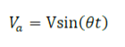
| It is assumed that the three-phase system is balanced: | ||||||||||||||||||||||||||||||||||||||||||
| These are the instantaneous phase voltages: | ||||||||||||||||||||||||||||||||||||||||||
 (2) (2) |
||||||||||||||||||||||||||||||||||||||||||
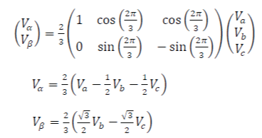
| When the three phase voltages are applied to a AC machine a rotating flux is created. This flux is represented as one rotating voltage vector. The magnitude and angle of this vector can be calculated with Clark's Transformation: | ||||||||||||||||||||||||||||||||||||||||||
 (3) (3) |
||||||||||||||||||||||||||||||||||||||||||
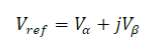
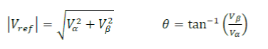
| The reference vector’s magnitude and angle is: | ||||||||||||||||||||||||||||||||||||||||||
 (4) (4) |
||||||||||||||||||||||||||||||||||||||||||
| The reference voltage can then be expresses as: | ||||||||||||||||||||||||||||||||||||||||||
 (5) (5) |
||||||||||||||||||||||||||||||||||||||||||
| The voltage vectors on the alpha and beta axis can then be described as: | ||||||||||||||||||||||||||||||||||||||||||
 (11) (11) |
||||||||||||||||||||||||||||||||||||||||||
| Having calculated Vα, Vβ, Vref and the reference angle, the first step is taken. The next step is to calculate the duration time for each vector V1-V6. | ||||||||||||||||||||||||||||||||||||||||||
| Time Duration | ||||||||||||||||||||||||||||||||||||||||||
| Switching Time Each sector having 7 switching states for each cycle. It starts and ends with a zero vector. The uneven numbers travel counter clockwise in each sector and the even sectors travel clockwise. The table3 shows the duty cycle of three phases that’s are, TA, TB, and TC for six sectors. | ||||||||||||||||||||||||||||||||||||||||||
SIMULATION RESULTS |
||||||||||||||||||||||||||||||||||||||||||
| The following results are done by works space model using MATLAB Simulink. And comparison of SPWM & SVPWM in THD level is following below. | ||||||||||||||||||||||||||||||||||||||||||
| A. Sinusoidal PWM | ||||||||||||||||||||||||||||||||||||||||||
| In SPWM, carrier based scheme is used for compare the reference wave(sine wave) with carrier wave in five level cascaded H- bridge inverter. | ||||||||||||||||||||||||||||||||||||||||||
| Phase Shifted Multi Carrier Modulation | ||||||||||||||||||||||||||||||||||||||||||
| The fig 9 shows the simulation results of cascaded 5 level H-bridge inverter using phase shifted modulation in SPWM. | ||||||||||||||||||||||||||||||||||||||||||
| Level Shifted Multi Carrier Modulation | ||||||||||||||||||||||||||||||||||||||||||
| In Phase Disposition | ||||||||||||||||||||||||||||||||||||||||||
| Alternative Phase Opposite Disposition | ||||||||||||||||||||||||||||||||||||||||||
| Phase Opposite Disposition | ||||||||||||||||||||||||||||||||||||||||||
| From these figures the In Phase Disposition method of Multi Carrier Modulation is better than other. These have low THD and better voltage. | ||||||||||||||||||||||||||||||||||||||||||
| B. Space vector PWM | ||||||||||||||||||||||||||||||||||||||||||
| The SVPWM has advantages than the SPWM .In this IPD Multi Carrier Modulation is used. This modulating wave is compared with the carrier wave the pulses are produced. That is given to the inverters gates. The phase voltage &line voltage wave of cascaded H- bridge 5 level inverter is following below. | ||||||||||||||||||||||||||||||||||||||||||
CONCLUSION |
||||||||||||||||||||||||||||||||||||||||||
| In this paper the comparison of SPWM &SVPWM with Cascaded H-bridge Five Level were discussed. And also discussed the types of multi carrier modulation. In that methods the in phase disposition method is better because of low THD (29.13%).then the space vector pulse width modulation having low THD (28.48%) compared to Sinusoidal Pulse Width Modulation.SVPWM have better DC utilization than SPWM.This simulation results were discussed using MATLAB simulink model. | ||||||||||||||||||||||||||||||||||||||||||
ACKNOWLEDGEMENT |
||||||||||||||||||||||||||||||||||||||||||
| Author would like to thank Mr. S.Veerakumar for their support in implementation of this project. | ||||||||||||||||||||||||||||||||||||||||||
Tables at a glance |
||||||||||||||||||||||||||||||||||||||||||
|
||||||||||||||||||||||||||||||||||||||||||
Figures at a glance |
||||||||||||||||||||||||||||||||||||||||||
|
||||||||||||||||||||||||||||||||||||||||||
References |
||||||||||||||||||||||||||||||||||||||||||
|


