Keywords
|
| CUK, Zeta, MIC (Multi-input DC-DC Converter), step-up and step-down conversion, duty ratio. |
| In the history of multi-input DC-DC converter for telecom power supplies, various converter combinations are being developed which are feasible for Telecom power supplies, where the demand of a wide range of power supplies is a very important feature, and giving the feasibility of either stepping up-down of voltages. The motto of this paper is to inculcate the available dc energy sources with existing topologies and meet the demands of the end user. The Telecom power supplies need electric energy sources with different electrical characteristics for meeting the needs of present day consumers. To provide such demands different sources along with combination of suitable converters led the way towards Multi-input DC-DC converters which are being considered as suitable alternatives for supplying the demanded loads [1]-[4]. Traditionally, two dc voltage sources are connected to two independent dc-dc power converters to obtain two stable and equivalent output voltages, which are then connected to the dc bus, to provide the electric energy demanded by the load. Another approach for the double-input dc-dc converter is to put two dc sources in series to form a single voltage source where traditional dc-dc power converters can be used to transfer power to the load. In order to transfer power individually, each dc voltage source needs a controllable switch to provide a bypass short circuit for the input current of the other dc voltage source to deliver electric energy continuously [3], [4]. Another approach is to put PWM converters in parallel with or without electrical isolation using the coupled transformer [5]. The schemes of control for these MICs with paralleled dc sources are based on the time-sharing concept because of the clamped voltage. Because of the voltage amplitude differences between two dc sources, only one of them can be connected to the input terminal of the dc-dc converter and transfer power to the load at a time [3]. |
INTRODUCTION
|
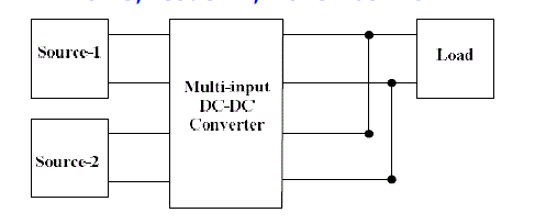
| The general form of a MIC consists of several input sources and a single load, conceptually shown in Fig. 1. In general, all of the input sources can deliver power to the load either separately or combinely. When only one of the input sources feeds the MIC, it will transfer power to the load individually and the MIC will operate as a PWM converter. In other words, when more than one input sources are supplied to the MIC, all input sources will deliver power to the load simultaneously without disturbing each other’s operation. The objective of this paper is to propose a double-input dc-dc converter which has the following advantages: The dc sources can deliver power to the load individually or simultaneously; the multi winding transformer is not needed; the magnitude of the input dc voltage can be higher or lower than the one with a regulated output; minimum switching devices are used in the converter circuit. The proposed double input dc-dc converter is proper for renewable-energy applications and combination of two different sources (such as battery and photo-voltaic or fuel cell). |
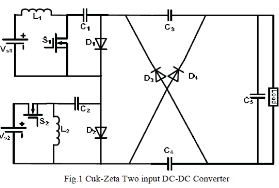
| The present day applications like Automotive Electric Vehicles, DC micro-grids, Photovoltaic based applications, Telecom power supplies all require converters which are capable of providing a wide range of power supplies. In this category, converters which are capable of providing the bucking as well as boosting feature are sought out to be the best options. In that particular category, converters which are having buck-boost feature is selected for performing the required operation. The proposed converter is integration of the CUK-Zeta converter combinations, resulting in the buck-boost operations. Though the combination will give a negative polarity towards the output side, proper care is taken to invert it, by using an additional cross diode-capacitor arrangement. |
CIRCUIT CONFIGURATION AND OPERATION PRINCIPLE OF THE PROPOSED CONVERTER
|
A. Cuk-Zeta Converter
|
| The integration of cuk-zeta converter combines the best qualities of both cuk and zeta converter. In this converter integration the order of converter is which has to be eight has been reduced to five, but inorder to invert the polarity of the conversion, and additional cross-capacitor diode bridge is being used which increases the order of converter to seventh order. By modifying the combination, and making a topological arrangement, an inductor is eliminated, without affecting the variation of the load ripple requirements. The converter is capable of being operated in both bucking as well as boosting mode of operation. Depending on the switching sequences the converter can be operated in four diffferent modes, but selective switching one mode is being eliminated. The converter combination has the added advantage of galvanic isolation, between input and output terminals and also the short circuits or other breakdown doesn't affect the sources. |
B. Circuit Configuration of Proposed Converter
|
| The schematic circuit diagram of the proposed double-input Cuk-Zeta dc-dc converter with two different voltage sources is shown in Fig. 2. It consists of two different input sources, Vg1 and Vg2, and four diodes, D1-D4, applied to provide a current path in different states. In this paper, permanent connection of input dc sources is considered, so S1 and S2 can be replaced with active switches if it’s required to connect and disconnect each of sources to input side of converter frequently. Energy receiver, converter and transmitter sections are situated in the middle side of the converter. This section is a two-port network that consists of a split-Capacitors C1 and C2 and diodes D1 and D2 connected in x-shape which is named “Cross diode-Capacitor network”. In this state, because both two sources are active, S1 and S2 are forward biased and S3 and D4 are reverse biased. |
1) State 1: Source 1and source 2 are active
|
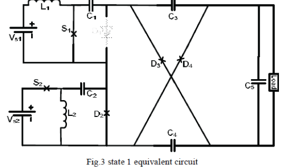
| The equivalent circuit of this state is shown in Fig. 3. In this state, source 1 and source 2 both are active, so only this mode capacitor C5 supplies the load requrement. In this mode the energy is stored in both the inductors L1 and L2. |
2) State 2, source 1 is active and source 2 is inactive
|
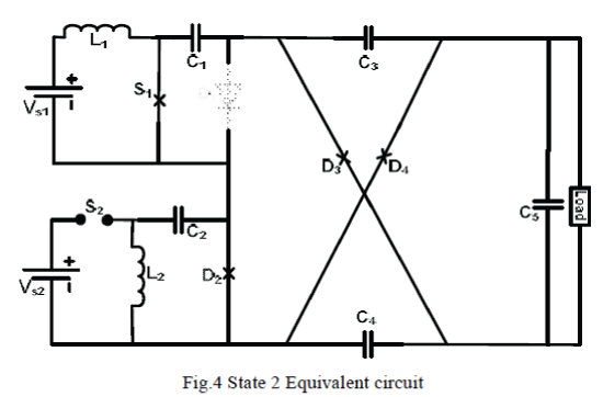
| In this mode still the inductor L1 is getting charged while source 2 is detached from the circuit because of the turning of switch S2, in this mode still the capacitor C5 supplies to the load. The local loop of C2, L2, D2 will try to charge the capacitor C2. |
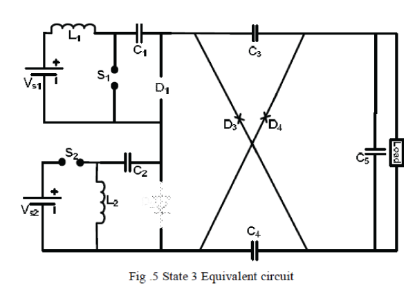
3) State 3: Source 1 is active and source 2 is inactive
|
| In this mode S1 is opened so the energy stored in inductor along with the source are now capable of driving the entire circuit, and source 2 is detached from the circuit. So the energy storage elements L1, L2, C1, C2 along with source-1, now feeds the load. |
| In all the modes the diodes D3 and D4 will be turned on, this ensure the reversal of current and there by the load always has the positve power supply of current throught the modes of operation. |
STEADY STATE ANALYSIS OF DOUBLE INPUT Z-SOURCE DC-DC CONVERTER
|
| Assuming that capacitors C1 and C2 have the same capacitance (C) , |
 |
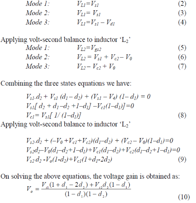
| By applying volt-second balance to inductor ‘L1’ & ‘L2’ we get the equations of ‘VL1’ applying volt-second balance to inductor ‘L1’ |
 |
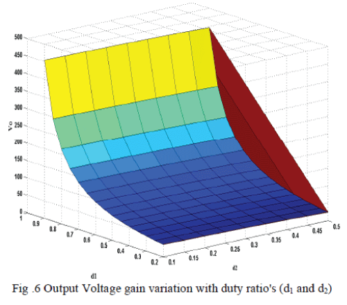
| By plotting the above equation, it can be verified that the proposed converter is having a wide output voltage range from a combination of different duty ratio's. It can be visualized in Fig. 6, that both the bucking as well as boosting of output voltage is possible by the proposed converter. |
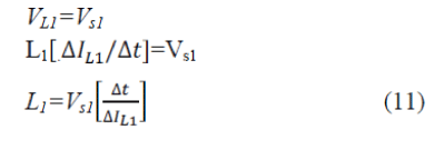
| Obtaining expressions for different components: |
 |
| Similarly Vs2=Vl2 |
 |
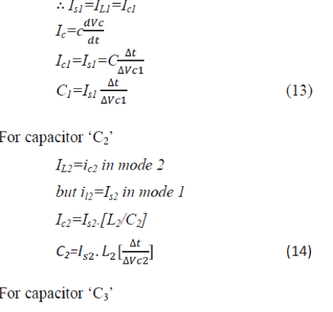
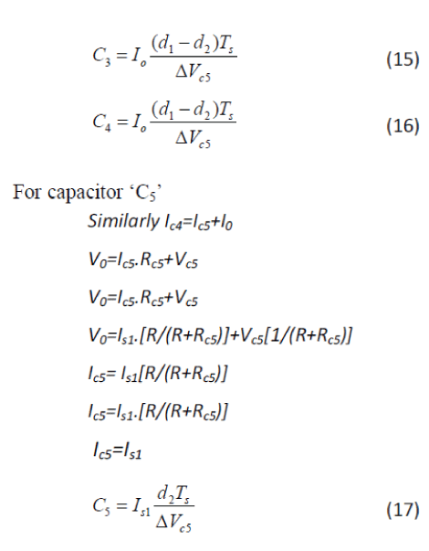
| For finding out capacitor values, we need KVL equations: |
| Applying KCL in fig4 first part for capacitor C1 |
| Let the current coming from source 1 let it be ‘Is’ |
 |
 |
SIMULATION RESULTS
|
| Simulation of the double input Cuk-Zeta dc-dc converter was performed using MATLAB/SIMULINK to confirm its operation the converter is simulated with the following parameters: |
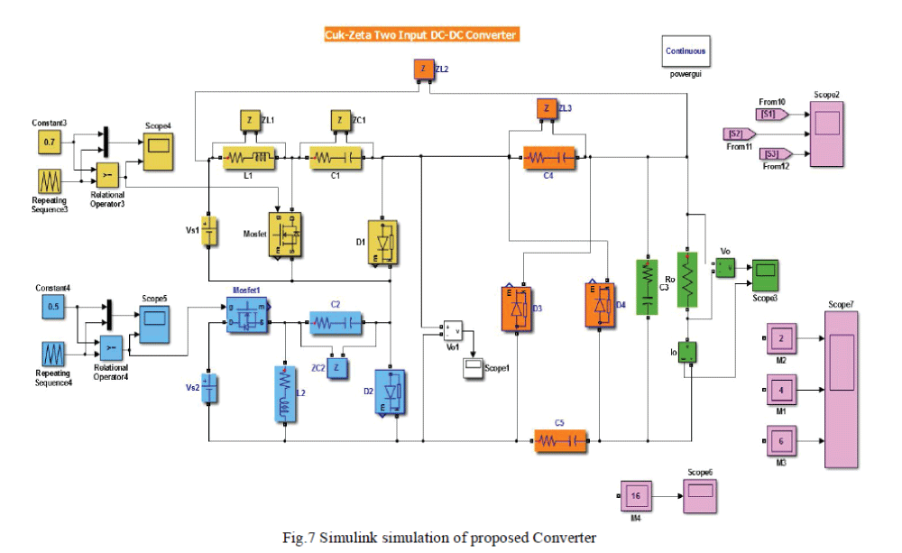
| The Matlab simulation of the proposed converter is shown in Fig. 7, for a given specification, the range of operation of duty cycles are found out, which are ranging from 0.1 to 0.4 for bucking operation, and 0.52 to 0.95 for boosting operation. |
| For analysis purpose, the source's voltages are taken as Vs1=24V, and Vs2=12V respectively. |
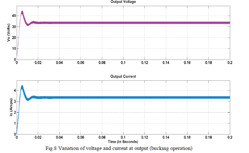
| The figure shown in Fig.8, gives the bucking mode of operation for already mentioned values of Vs1 and Vs2. The output voltage is got as 33V, for a duty ratio of d1=0.1, and d2=0.44. The output voltage is less than the combined voltage of the two sources. |
| The figure shown in Fig.9, gives the boosting mode of operation of proposed converter for already mentioned values of Vs1 and Vs2. The output voltage is got as 190V, for a duty ratio of d1=0.88, and d2=0.72. The output voltage boosted to around four times. |
| The waveform shown in the Fig. 10, are the variations of various currents through different energy storage elements, when they are being operated in bucking mode of operation, for roughly understanding their behavior, during inital transient period and the steady state operating region. |
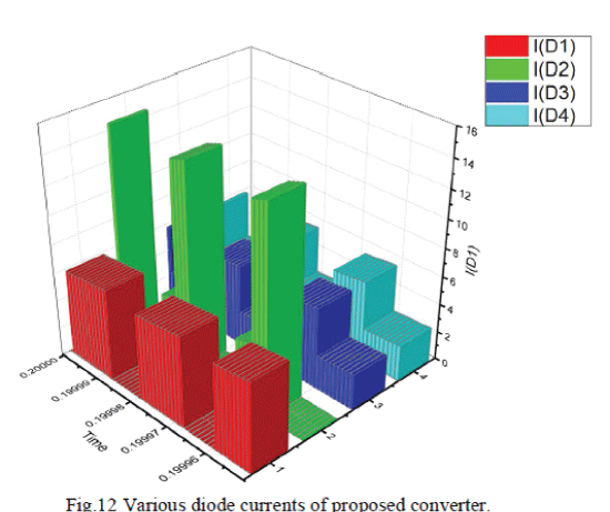
| The bar-graph shown in Fig. 12, shows that the variation of current through different diodes present in the topology, since they are responsible for communicating the sources to the load, the amount of current they carry gives the idea of fixing the suitable range of current and voltage rating, thereby their protection and operation abnormalities can be viewed. |
CONCLUSION
|
| In this paper, a new double input Cuk-zeta dc-dc converter is proposed. The operation principle, and steady-state analysis is explained in detail. The analysis and simulation results show the input dc sources can deliver power to the load, as failure of each input sources doesn’t disturb the other’s operation. Two input sources can have different characteristics and voltage. The capability of the proposed converter being operated both in bucking and boosting mode is an advantageous feature. Boosting feature of converter makes it proper for new energy applications. The converter may be further investigated for dynamic analysis. The closed loop conrol strategy may also be implemented for the proposed converter. |
Tables at a glance
|
 |
 |
| Table 1 |
Table 2 |
|
| |
Figures at a glance
|
 |
 |
 |
 |
| Figure 1 |
Figure 2 |
Figure 3 |
Figure 4 |
|
 |
 |
 |
 |
| Figure 5 |
Figure 6 |
Figure 7 |
Figure 8 |
|
 |
 |
 |
| Figure 11 |
Figure 12 |
Figure 13 |
|
| |
References
|
- E. Muljadi and H. E. McKenna, “Power quality issues in a hybrid power system,” IEEE Trans. Ind. Appl., vol. 38, no. 3, pp. 803-809, May/Jun 2002.
- F. Giraud and Z. M. Salameh, “Steady-state performance of a gridconnected rooftop hybrid wind-photovoltaic power system with battery storage,” IEEE Trans. Energy Convers., vol. 16, no. 1, pp. 1-7, Mar 2001.
- Yaow-Ming Chen, Yuan-Chuan Liu, and Sheng- sien Lin, “Double- Input PWM DC-DC Converter for High-/Low-Voltage Sources,” IEEE Trans. Ind. Electron., vol. 53, no. 5, October 2006.
- Yuan-Chuan Liu and Yaow-Ming Chen, “A systematic approach to synthesizing multi-input dc–dc converters” IEEE Trans. Power Electron., vol. 24, no. 1, January 2009.
- H. Matsuo,W. Lin, F. Kurokawa, T. Shigemizu, and N.Watanabe, “Characteristics of the multiple-input dc-dc converter,” IEEE Trans. Ind. Electron., vol. 51, no. 3, pp. 625-631, Jun 2004.
- F. Z. Peng, “Z-Source inverter,” IEEE Trans. Ind. Appl., vol. 39, no. 2,pp. 504-510, March/April 2003.
- Xu Peng Fang, Zhao Ming Qian, and Fang Zheng Peng, “Single-phase Z-Source PWM AC-AC Converters,” IEEE Power Electron. Lett., vol. 3, no. 4, December 2005.
- E. Licéaga-Castro, C.E. Ugalde-Loo, J. Licéaga-Castro, and P. Ponce. “An efficient controller for SV-PWM VSI based on the multivariable structure function”. To be presented at: 44th IEEE CDC-ECC, Spain, 2005.
- C.E. Ugalde-Loo. Control de motores de inducción utilizando la función de estructura multivariable. MSc. Dissertation. IPN SEPI ESIME, 2005.
|
