International Journal of Advanced Research in Electrical, Electronics and Instrumentation Engineering
ISSN ONLINE(2278-8875) PRINT (2320-3765)
ISSN ONLINE(2278-8875) PRINT (2320-3765)
M. Vijaya Kumar1, K. Babu2,K. Guna Prasad3, R. Ramesh4
|
| Related article at Pubmed, Scholar Google |
Visit for more related articles at International Journal of Advanced Research in Electrical, Electronics and Instrumentation Engineering
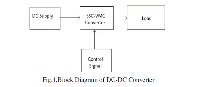
Now-a-days the new family of dc-dc converters based on three state switching cell and voltage multiplier cells. It present a demonstrate of some advantages and limitations of a several topologies were typically use in voltage step-up applications. The operating principle of this family has chosen the boost converter and discussed in detail. The analysis of converter can applicable in uninterruptible power supplies, fuel cell systems and it is adequate in operating the high-gain boost stage with cascaded inverters in the renewable energy systems. Furthermore, It is applicable in dc voltage step-up is demanded, like electrical fork-lift, audio amplifiers, and some other applications.
Keywords |
| dc-dc converters, voltage gain, voltage number cells (VMCs), Boost converters |
INTRODUCTION |
| Depending on the appliance nature, many kinds of static power converters are necessary for the adequate conversion and acquisition of the energy provided by primary sources like electrical phenomenon arrays, wind turbines, and fuel cells. Besides, considering that the price of renewable energy systems is high, the utilization of high-efficiency power electronic converters may be a should. |
| The need for solid-state ac–dc converters to enhance power quality in terms of power factor correction, minimized over all harmonic distortion at input ac mains, and exactly regulated dc output has intended the investigation of many topologies supported classical converters like buck, boost, and buck–boost converters. Boost converters operative in continuous-conduction mode became particularly fashionable because reduced magnetic attraction interference levels result from their utilization.. The approach additionally employs the principle of interleaved converters, because it is extended to a generic range of legs per winding of the autotransformers and high power levels. |
| A three-state switching cell (3SSC) can be obtained by the association of two two-state switching cells (2SSCs) interconnected to a center-tapped autotransformer, from which a family of dc–dc converters can be derived. This concept was first introduced in, as the so-called cell type B is obtained. The first topology for PFC applications based on the 3SSC was introduced. It can be obtained by replacing the input source of the dc–dc boost converter presented in by a typical single-phase diode bridge and an ac voltage source. The presence of the diode bridge causes conduction losses to increase because the current always flows through four semiconductor elements. Attempts to achieve high output voltage gain using the 3SSC and the dc–dc boost converter were performed. Although only two diodes and two capacitors are added to the original topology, the extension to PFC applications with high efficiency is limited by the presence of increased number of components in the current path during each operating mode. This mode is also called boundary conduction mode because it represents the intermediate operation between CCM and discontinuousconduction mode (DCM). The analysis of the critical conduction mode (CRM) is based on the study developed for the previous conduction modes and is required so that the static characteristic of the converter operating in NOM is determined. In this case, the minimum current through Lb is null, i.e., the current through Lb is equal to zero for a single time instant. The ripple current through Lb is then equal to the maximum current IM. |
 |
| For good operation of the VMC ac input voltage is required, which is an important requirement of this cell. Due to this fact, the use of the 3SSC depicted is considered because it generates such ac voltage across the terminals of the autotransformer and therefore the drain terminals of the controlled switches. Within the ensuing cell, the controlled switches may be described by MOSFETs, junction field-effect transistors, insulated gate bipolar transistors, bipolar junction transistors, etc. Completely the generated topologies gift bifacial characteristics. As was mentioned before, the utilization of high-voltage gain converters is of nice interest, although several approaches are supported isolated topologies. it's price value that the utilization of non-isolated converters significantly dedicated to applications relating to renewable power systems has been the scope of recent works. The efforts resulting in the event of such non-isolated topologies area unit then well even within the literature. |
LITERATURE SURVEY |
| Title: An improved maximum power point tracking for photovoltaic grid-connected inverter based on voltage-oriented control |
| Author: R. Kadri, J.-P. Gaubert, and G. Champenois, |
| Publish: IEEE, vol. 58, no. 1, pp. 66–75, Jan. 2011. |
| An improved maximum power point (MPP) tracking (MPPT) with better performance based on voltageoriented control (VOC) is proposed to solve a fast changing irradiation problem. In VOC, a cascaded control structure with an outer dc link voltage control loop and an inner current control loop is used. The currents are controlled in a synchronous orthogonal d, q frame using a decoupled feedback control. |
| Title: Class-D audio amplifiers in mobile applications |
| Author: M. Berkhout and L. Dooper, |
| Publish: IEEE, vol. 57, no. 5, pp. 992–1002, May 2010. |
| A comparative system-level overview is given of alternative class-D amplifier architectures. The theory behind pulse width modulation and different modulation schemes is discussed. Topological alternatives such as open-loop versus feedback and fixed-carrier versus self-oscillating are analyzed and compared in terms of relevant characteristics, such as distortion, power supply rejection, efficiency, and electromagnetic interference. The combination of digital-to-analog conversion and class-D amplifiers is discussed. |
| Title: Highly efficient high step-up converter for fuel-cell power processing based on threestate commutation cell |
| Author: S. V. Araujo, R. P. Torrico-Bascope, and G. V. Torrico-Bascope, |
| Publish: IEEE, vol. 57, no. 6, pp. 1987–1997, Jun. 2010. |
| The modification of a boost converter operating with a three-state commutation cell that is already well suited for high current stress in the input due to the current sharing between the active switches. |
MODULATION SRATEGIES |
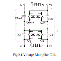
| Voltage multiplier Cell |
| A voltage multiplier factor is an electrical circuit that converts AC power from a lower voltage to a better DC voltage, usually employing a network of capacitors and diodes. Voltage multipliers are often used to generate some volts for electronic appliances, to many volts for functions like high-energy physics experiments and lightning safety testing. |
 |
 |
 |
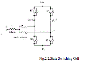
State switching cell |
| The 3SSC is obtained by the association of switching two-state change PWM cells (2SSCs) interconnected to a center faucet autotransformer, from which a family of dc–dc converters are often derived. a new non-isolated bidirectional device is proposed on this work. This converter stage is appropriate for applications of DC and AC motor drives. During this device, for a given duty cycle, the output to input voltage ratio will be raised by adding transformer turns ratio. Another necessary feature of this device is that the lower blocking voltage across the controlled switches compared to similar circuits, that permits the use of MOSFETs switches with lower conductivity resistances RDS (on). Co-occurring or later production of electronic product, and (3) conformity of favor throughout a conference proceedings. Margins, column widths, line spacing, kind and designs are built-in; samples of the kind designs are provided throughout this document and are known in italic type, at intervals parentheses, following the instance. Some elements, like multi-leveled equations, graphics, and tables aren't prescribed, though the assorted table text designs are provided. The formatter can got to produce these elements, incorporating the applicable criteria that follow. |
Operating Principle |
| Switches S1 and S2 are turned ON, whereas all diodes are reverse biased. Energy is kept in inductance L and there's no energy transfer to the load. The output capacitor provides energy to the load. This stage finishes once switch S1 is turned OFF. |
| Switch S1 is turned OFF, whereas S2 remains turned ON and diodeD5 is conducted. There is no energy allocation to the load also. Inductor L stores energy, capacitors C1 and C3 are discharged, and capacitors C2, C4, andC6 are charged |
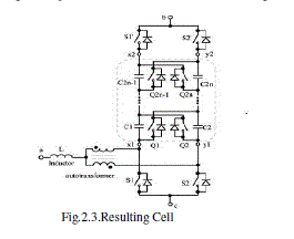
PROPOSED TOPOLOGIES |
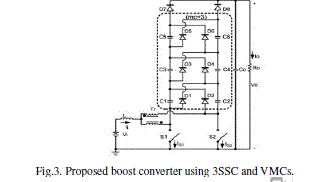
| The developed analysis considers the device related to three voltage multiplier cells and is elaborated as follows. |
| In order to raised perceive the in operation principle of the |
| Structures, the subsequent assumptions are made: |
| 1) The input voltage is less than the output voltage |
| 2) Steady-state operation is taken into account |
| 3) Semiconductors and geophysics are ideals |
| 4) Change frequency is constant; |
| 5) The turn’s ratio of the autotransformer is unity; |
| 6) The drive signals useful to the switches are 180âÃâæExiled. |
Operating principle |
| The pattern that uses three multiplier cells is defined in Fig. 3. The comparable circuits that match up to the device process given in Figs. 4 correspondingly. |
 |
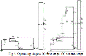 |
| First stage [t0,t 1] [see Fig. 4(a)]: Switches S1 and S2 are turned ON, whereas all diodes are reverse biased. Energy is kept in inductance L and there's no energy transfer to the load. The output capacitor provides energy to the load. This stage finishes once switch S1 is turned OFF. |
| Second stage [t1,t2] [see Fig. 4(b)]:switch S1 is turned OFF, whereas S2 remains turned ON and diodeD5 is forward biased. There’s no energy transfer to the load also. Inductor L stores energy, capacitors C1 and C3 area unit discharged, and capacitors C2, C4, and C6 are charged. |
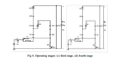 |
| Third stage [t2,t3] [see Fig. 4(c)]:switches S1 and S2 stay turned OFF and ON, respectively. Diodes D3 and D7 are forward biased, whereas all the outstanding ones are reverse biased. Energy is transmitted to the output stage over D7.The inductor stores energy and capacitors C2 and C4 are still charged. Capacitors C1 is discharged, and then are C3 and C5. |
| Fourth stage [t3,t4] [see Fig. 4(d)]:clarifies the switch S2 remainders turned ON, diode D3 is inverse biased, and diode D1 is forward biased. Energy is conveyed to the load over D7. The inductor is discharged, and then are capacitors C1, C3, and C5, whereas C2 is charged |
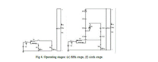 |
| Fifth stage [t4, t5 ] [see Fig. 4(e)]: This stage is identical to the first one. |
| Sixth stage [t5, t6 ] [see Fig. 4(f)]: Switch S2 is turned OFF and switch S1 is being turned ON. Diode D6 is onward biased. The inductance is charged by the input source, although capacitors C2 and C4 are discharged instead. |
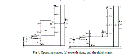 |
| Seventh stage [t6, t7 ] [see Fig. 4(g)]: This stage is similar to the third one. |
| Eighth stage [t7, t8] [see Fig. 4(h)]: Switch S1 is turned ON, while S2 remains turned OFF. Diodes D2 and D8 are forward biased, while D4 is reverse biased as well as the remaining diodes. Energy transfer to the load occurs through D8, and capacitor Co is being charged. The inductance is discharged, while capacitor C1 is charged then capacitors C2, C4, and C6 remain discharged. |
Static Gain |
| The static gain for the generic structure of the boost converter can be obtained from the inductor volt–second balance. The voltage range increased by the time interval that agrees to the inductor charge is equal to that regarding the inductor discharged. |
 |
SIMULATION RESULTS |
| MATLAB/SIMULINK is used for the simulation studies. Fig 5 shows the simulation circuit of High Voltage Gain DCDC Converters Based On 3SSC and VMC Using Non-isolated Converter |
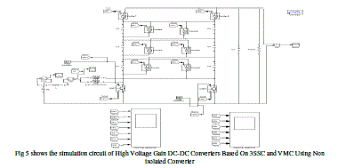 |
| The above fig.5 shows the simulation diagram for the proposed boost converter based on 3SSCand VMC in these simulation switches S1and S2 are taken as MOSFET’s and then VMC can going to add the voltage levels at three stages and it produce the output voltage as 450V in these we are giving the input voltage as 42V-54V based on the specifications we are going to give the input supply. |
 |
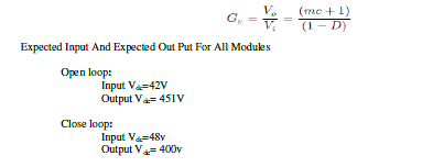
| The above fig. 6 shows the output DC voltage of the boost converter based on 3SSC and VMC in the open loop circuit as the supply we are going to give the source 48V we are going to get the 455V output supply has been presented in the system . |
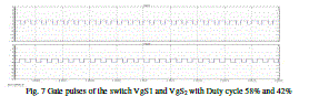 |
| The above fig. 7 shows the gating pulses across the switches to the system when the frequency has been applied to 25KHZ at that time we are getting 58% of Duty cycle has been presented it is in ON position remaining part is in OFF position it shows 42% of Duty cycle. |
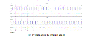 |
| The above fig. 8 shows the voltages were presented across the switches of the MOSFET’s were S1 and S2has been presented in the wave from. |
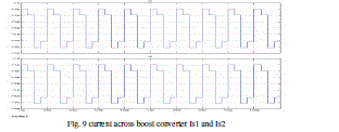 |
| The above fig. 9 shows the current wave forms were it presented across the boost converter switches of the MOSFET’s it going to be presented and it show the Is1 and Is2. |
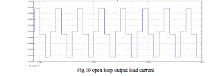 |
| The above fig. 10 shows the output load current across the load terminals of the output side as it present the load current it shows the pulse wave as peak to peak of the terminals as it presented. |
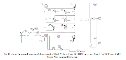 |
| The above fig. 11 shows the closed loop circuit diagram of the proposed converter of the 3SSC and VMC by placing the PID controllers across the switches S1 and S2 of the boost converter and we are giving the source as 48V then we are getting the 400V output as we are already mention the reference value as 400V by that it going to calculate and it going to present the output wave form of the system. |
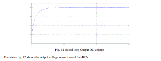 |
| The above fig. 12 shows the output voltage wave form of the 400V |
CONCLUSION |
| Six generalized non isolated high gain voltage dc–dc converters. To verify the principle operation of the generated structures, the boost converter was chosen. The topology is adequate for several applications such as photovoltaic systems, fuel cell systems, and UPSs, where high voltage gain between the input and output voltages are demanded. |
References |
|