ISSN ONLINE(2278-8875) PRINT (2320-3765)
ISSN ONLINE(2278-8875) PRINT (2320-3765)
Arathy M1, Sreekala P2
|
| Related article at Pubmed, Scholar Google |
Visit for more related articles at International Journal of Advanced Research in Electrical, Electronics and Instrumentation Engineering
The conventional power conditioning units require a DC-DC converter followed by an inverter circuit to deliver the required power to the load. This increases the required power conversion stages, system cost, size and reduces the overall system efficiency. This paper presents a boost converter topology that provides DC-AC conversion along with voltage boosting in a single stage. The multi level differential boost converter topology consists of two boost converters connected back to back with a voltage boosting function. Multi level differential boost converter topology requires less power conversion stages and reduces the size of power conditioning units. This converter topology can be employed in uninterruptible power supplies and AC drives. With the differential boost converter topology, a ripple free pure sinusoidal wave can be obtained. The differential boost converter topology provides a multi level output along with voltage boosting by employing a single DC voltage source. The design and analysis of multi level differential boost converter have been done.
Keywords |
| Multilevel differential Boost Converter, Boost converter, PV panel. |
INTRODUCTION |
| The demand for renewable energy sources has increased with increase in the rate of power failures. The solar irradiation does not remains constant throughout the day. So we have to employ Maximum Power Point Techniques (MPPT) for the effective utilization of solar power. |
| Conventional Switched-Mode Power Converters (SMPC) convert the voltage input to another voltage signal. Power is controlled by controlling the timing that the electronic switches are “on” and “off”. Power electronic devices are mainly used in computers, electronic equipments, uninterruptible power supplies, telecommunication systems, etc. Power conditioning units require a DC- DC converter followed by a DC- AC inverter to deliver the required power to the load. The current paper focuses on the development of a multilevel differential boost converter topology that provides an AC output voltage in a single stage to reduce the switching losses and improve the efficiency of the power conditioning unit. |
| For tracking maximum power from a PV panel, a SEPIC or Cuk converter was placed between a solar panel and the load. This method used pulse width modulated control scheme. The proposed method does not require complex mathematical calculations [1]. Perturb & Observe (P & O) algorithm cannot identify the variations of the photovoltaic array output due to duty cycle modulation from those ones due by the irradiance variation. This drawback of P & O algorithm can be improved by changing the value of the duty cycle variations to the dynamic response of the DC-DC converter [2]. The conventional DC-DC converters increase the input current ripple. This can be reduced by implementing a combinational circuit of Boost and Buck-Boost DC-DC Converter connected in series. The proposed converters operate in alternate fashion and limit the input ripple current [3]. For the effective utilization of solar power, different types of power tracking methods are employed. Different studies were conducted to compare and study the MPPT methods along with the factors to be considered while selecting a MPPT technique. The advantages of P&O algorithm and PSO algorithm can be combined to develop a new method for MPPT [4,10]. Among the different MPPT methods, the most commonly used MPPT algorithms are P & O algorithm and IC algorithm. A comparative study between these two algorithms on buck converter, boost converter and cuk converter revealed that even though IC algorithm could track maximum power under fast varying atmospheric conditions, it increased the circuit complexity |
| when compared with P & O algorithm. By doing simulation studies with IC controller and P & O controller on buck, boost and cuk converter, IC controller was found to be a better MPPT controller when compared with P&O [5]. Later fuzzy algorithm and MPPT controller was implemented on DC-DC Boost converter. This simplified DC-DC converter topology. This system when compared with existing systems is more efficient and tracks the maximum power effectively from solar cell into battery [6, 9, 11]. P & O algorithm based on variable step overcomes the disadvantages of the duty cycle perturbation based on fixed-step, and it provides maximum power point tracking [7]. The interleaved boost converters can be employed to reduce the input ripple current, improve system efficiency, reliability and reduce electromagnetic emission [8]. Self lift cuk converter, an improved version of the cuk converter can reduce the output voltage ripple, current stress, voltage stress and switching losses [12]. |
| All these converter circuits could only convert the DC voltage from one level to another level. They cannot provide the AC voltage required to feed AC loads in a single stage. This increased the power conversion stages, cost and affected the efficiency of power conditioning units. Differential boost converter overcomes the disadvantages of conventional converter circuits. They reduce the power conversion stages and the the overall size of the power conditioning units |
DIFFERENTIAL BOOST CONVERTER |
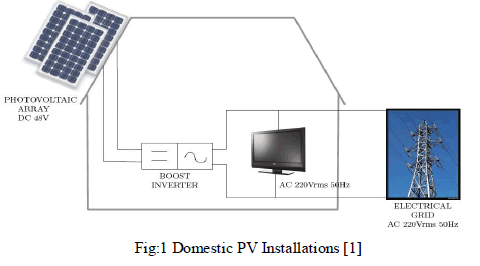
| A boost circuit is a DC-DC converter. It provides an output voltage larger than its input voltage. Alternating current cannot be generated with this converter. For this, an inverter is developed by duplicating the boost converter circuit [13]. Fig: 1 shows the application of differential boost converter for PV installations. |
 |
| A differential boost converter consists of two boost converters connected back to back with a voltage boosting function. Each boost converter produces a DC biased sinusoidal output voltage V1 and V2 with a phase shift of 1800. This maximizes the output voltage across the load. Fig: 2 show the block diagram description of a differential boost converter. Converter A is for the positive converter and the converter B for the negative group. Differential boost converter employs two symmetrical circuits with the load R connected across the converters A and B. |
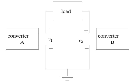 |
| Fig:2 Block diagram of differential boost converter[2] |
METHODOLOGY |
| Methodology mainly comprises of design of the five level differential boost converter for voltage inversion. The input to the multilevel differential boost converter can be either from a 12 V 7 Ah battery or from a PV panel. If PV panel is employed as the power source, a boost converter should be provided for converting the unregulated output voltage of PV panel to regulated output voltage. The five level differential boost converters is used to drive an induction motor |
A. Design of differential boost converter |
| The assumptions to be considered while designing a boost converter are as follows |
| 1. All the elements are ideal and the current is assumed to be continuous. |
| 2. The supply voltage is constant |
| 3. The converter operates at high switching frequency |
| 4. The inductance and capacitance are equal and symmetric. |
| 5. V1 and V2 are of equal magnitude and sinusoidal |
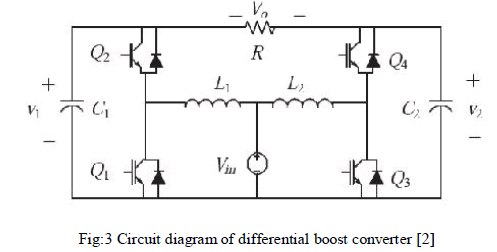
| Fig:3 shows the circuit diagram of differential boost converter. In the circuit, Vin is the input voltage, L1 and L2 are the energy storage capacitors and C1 and C2 are the filtering capacitors. R is the load connected across the two boost converters. V1 and V2 are the output voltages of the two boost converters. There are two modes of operation for the differential boost converter. |
 |
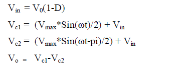
| The equations for the design of differential boost converter are exactly similar to the design of a conventional boost converter circuit with Vo as the output voltage, D as the duty cycle of the boost converter and Vin, the converter input voltage. Assume the value of capacitors equal to 150 μF. The design equations employed are as follows |
 |
| At unity power factor, the output current of the differential boost converter is |
 |
| By employing eqns 1, 2, 3 and 5 , the value of the inductors employed is calculated using eqn 8 |
| Where f is the required frequency of the output AC voltage. |
| The modified differential boost converter circuit for obtaining the required output employs 6 switches. |
SIMULATION AND RESULTS |
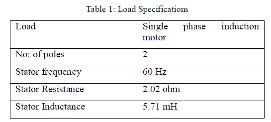
| The PV powered five level inverter using differential boost converter is simulated in matlab/simulink software. The control algorithm implemented is sinusoidal pulse width modulation. The boost converter is employed to provide a stable DC bus. The output voltage of the multi level differential boost converter is used to drive a single phase induction motor. The prototype and specifications of the single phase induction motor drive is given in table 1. |
 |
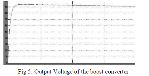
| Fig 5 shows the output voltage of the boost converter employed to provide a stable DC bus. |
 |
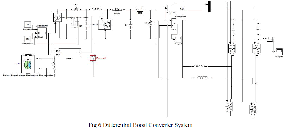
| Fig:6 is the simulink implementation of the five level inverter implemented using multilevel differential boost converter. |
 |
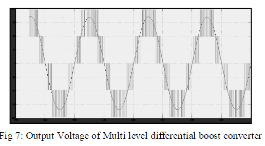
| Fig 7 is the output voltage of the five level inverter implemented using differential boost converter |
 |
| Fig: 8 shows the speed curve of the induction motor employed as load. |
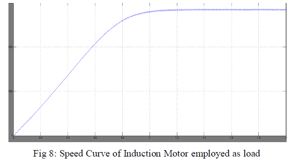 |
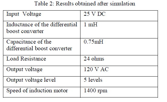
| From the simulation results, it was found that multi level differential boost converter can be employed to feed an AC motor drive. The multi level differential boost converter topology provides the AC output voltage in a single stage and reduce the power conversion stages required in power conditioning units. The speed of the induction motor drive obtained is 1400 rpm. The input and output voltages of the differential boost converter obtained during simulation and values of the inductances and capacitances are given in table 2. |
 |
CONCLUSION |
| With the multilevel differential boost converter topology, the power conversion stages required in conventional power conditioning units get reduced. Multi level differential boost converter topology provided DC-AC conversion along with voltage boosting function in a single stage. This minimized the power conversion losses, reduced size and cost of power conditioning units. The new converter topology can be employed in uninterruptible power supplies and AC drives to reduce overall system size. With the differential boost converter topology, a ripple free pure sinusoidal wave can be obtained. The differential boost converter topology provides a five level or seven level output along with voltage boosting in a single stage with a single DC voltage source. The analysis of multilevel differential boost converter feeding an induction motor drive has been done in Matlab/Simulink. |
References |
|