ISSN ONLINE(2278-8875) PRINT (2320-3765)
ISSN ONLINE(2278-8875) PRINT (2320-3765)
Pankaj H Zope1, Pravin G.Bhangale2, Prashant Sonare3 ,S. R.Suralkar4
|
| Related article at Pubmed, Scholar Google |
Visit for more related articles at International Journal of Advanced Research in Electrical, Electronics and Instrumentation Engineering
SPWM or sinusoidal pulse width modulation is widely used in power electronics to digitize the power so that a sequence of voltage pulses can be generated by the on and off of the power switches. The pulse width modulation inverter has been the main choice in power electronic for decades, because of its circuit simplicity and rugged control scheme SPWM switching technique is commonly used in industrial applications SPWM techniques are characterized by constant amplitude pulses with different duty cycle for each period. The width of this pulses are modulated to obtain inverter output voltage control and to reduce its harmonic content. Sinusoidal pulse width modulation or SPWM is the mostly used method in motor control and inverter application. In this development a unipolar and bipolar SPWM voltage modulation type is selected because this method offers the advantage of effectively doubling the switching frequency of the inverter voltage, thus making the output filter smaller, cheaper and easier to implement. Conventionally, to generate this signal, triangle wave as a carrier signal is compared with the sinusoidal wave, whose frequency is the desired frequency. In this paper single-phase inverters and their operating principles are analyzed in detail. The concept of Pulse Width Modulation (PWM) for inverters is described with analyses extended to different kinds of PWM strategies. Finally the simulation results for a single-phase inverter (unipolar) using the PWM strategies described are presented [1],[2],[3]. Index Term—Modulation, Sinusoidal pulse width modulation, Unipolar, Bipolar
Index Term |
| Modulation, Sinusoidal pulse width modulation, Unipolar, Bipolar |
INTRODUCTION |
| The dc-ac converter, also known as the inverter, converts dc power to ac power at desired output voltage and frequency. The dc power input to the inverter is obtained from an existing power supply network or from a rotating alternator through a rectifier or a battery, fuel cell, photovoltaic array or magneto hydrodynamic generator. The filter capacitor across the input terminals of the inverter provides a constant dc link voltage. The inverter therefore is an adjustable-frequency voltage source. The configuration of ac to dc converter and dc to ac inverter is called a dc-link converter. [2] Inverters can be broadly classified into two types, voltage source and current source inverters. A voltage–fed inverter (VFI) or more generally a voltage–source inverter (VSI) is one in which the dc source has small or negligible impedance. The voltage at the input terminals is constant. A current –source inverter (CSI) is fed with adjustable current from the dc source of high impedance that is from a constant dc source [2]. A voltage source inverter employing thyristor as switches, some type of forced commutation is required, while the VSIs made up of using GTOs, power transistors, power MOSFETs or IGBTs, self commutation with base or gate drive signals for their controlled turn-on and turn-off. A standard single-phase voltage or current source inverter can be in the half-bridge or fullbridge configuration. The single-phase units can be joined to have three-phase multiphase topologies. Some industrial applications of inverters are for adjustable-speed ac drives, induction heating, standby aircraft power supplies, UPS (uninterruptible power supplies) for computers, HVDC transmission lines, etc [1],[8]. |
| This paper is organized as: In section I explain the basic inverter types. Section II includes simple different PWM techniques. section III explain SPWM techniques. Here in sectionIV explains Implemented results and Simulated result for only unipolar voltage switching for fixed modulation index (m=0.6) |
A.INVERTERS (INTRODUCTION) |
| A device that converts DC power into AC power at desired output voltage and frequency is called an Inverter. Phase controlled converters when operated in the inverter mode are called line commutated inverters. But line commutated inverters require at the output terminals an existing AC supply which is used for their commutation.This means that line commutated inverters can’t function as isolated AC voltage sources or as variable frequency generators with DC power at the input. Therefore, voltage level, frequency and waveform on the AC side of the line commutated inverters can’t be changed. On the other hand, force commutated inverters provide an independent AC output voltage of adjustable voltage and adjustable frequency and have therefore much wider application.[13] |
| Inverters can be broadly classified into two types based on their operation: |
| Voltage Source Inverters(VSI) |
| Current Source Inverters(CSI) |
| Voltage Source Inverters is one in which the DC source has small or negligible impedance. In Other words VSI has stiff DC voltage source at its input terminals. A current source inverter is fed with adjustable current from a DC source of high impedance, i.e; from a stiff DC current source. In a CSI fed with stiff current source, output current waves are not affected by the load. From view point of connections of semiconductor devices, inverters are classified as under [1],[2] |
| Bridge Inverters |
| Series Inverters |
| Parallel Inverter |
| Bridge Inverters are classified as |
| Half bridge |
| Full bridge |
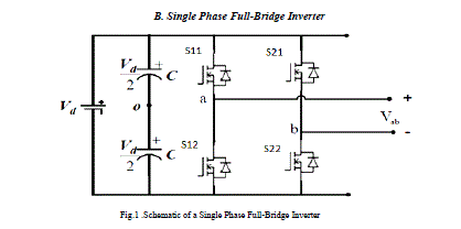 |
| A single-phase inverter in the full bridge topology is as shown in Fig. 1 which consists of four switching devices, two of them on each leg. The full-bridge inverter can produce an output power twice that of the half-bridge inverter with the same input voltage. The S PWM switching schemes are discussed in this section, which improve the characteristics of the inverter. The objective is to add a zero sequence voltage to the modulation signals in such a way to ensure the clamping of the devices to either the positive or negative dc rail; in the process of which the voltage gain is improved, leading to an increased load fundamental voltage, reduction in total current distortion and increased load power factor. In Fig. 1, the top devices are assigned to be S 11 and S 21 while the bottom devices as S 12 and S 22, the voltage equations for this converter are as given in the following equations.[ 1] |
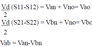 |
| The voltages Van and Vbn are the output voltages from phases A and B to an arbitrary point n, Vno is the neutral voltage between point n and the mid-point of the DC source. The switching function of the devices can be approximated by the Fourier series to be equal to 1/2 * M.Where M is the modulation signal which when compared with the triangular waveform yields the switching pulses Thus from Equations1, 2, and 3 the expressions for the modulation signals are obtained as |
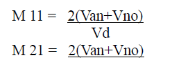 |
| Equations 4 and 5 give the general expression for the modulation signals for single-phase dc-ac converters. The various types of modulation schemes presented in the literature can be obtained from these equations using appropriate definition for Van, Vbn &Vno[1] |
RESEARCH METHODOLOGY (DIFFERENT PWM TECHNIQUES FOR SINGLE PHASE INVERTER) |
A. Single pulse width modulation |
| In this control, there’s only one pulse per half cycle and the width of the pulse is varied to control the inverter output. The gating signals are generated by comparing a rectangular reference signal of the amplitude Ar with triangular carrier wave of amplitude Ac, the frequency of the carrier wave determines the fundamental frequency of output voltage. By varying Ar from 0 to Ac, the pulse width can be varied from 0 to 100 percent. The ratio of Ar to Ac is the control variable and defined as the modulation index.[1],[2],[5]. |
B. Multiple pulse width modulation |
| The harmonic content can be reduced by using several pulses in each half cycle of output voltage. The generation of gating signals for turning ON and OFF transistors by comparing a reference signal with a triangular carrier wave. The frequency Fc, determines the number of pulses per half cycle. The modulation index controls the output voltage. This type of modulation is also known as uniform pulse width modulation (UPWM).[1],[2]. |
C. Sinusoidal pulse width modulation (SPWM) |
| Instead of, maintaining the width of all pulses of same as in case of multiple pulse width modulation, the width of each pulse is varied in proportion to the amplitude of a sine wave evaluated at the centre of the same pulse. The distortion factor and lower order harmonics are reduced significantly. The gating signals are generated by comparing a sinusoidal reference signal with a triangular carrier wave of frequency Fc.The frequency of reference signal Fr ,determines the inverter output frequency and its peak amplitude Ar,controls the modulation index M,and Vrms output voltage VO.The number of pulses per half cycle depends on carrier frequency .[1],[13]. |
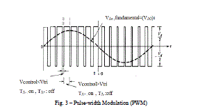
| Inverters that use PWM switching techniques have a DC input voltage that is usually constant in magnitude. The inverters job is to take this input voltage and output ac where the magnitude and frequency can be controlled. There are many different ways that pulse-width modulation can be implemented to shape the output to be AC power. A common technique called sinusoidal- PWM will be explained. In order to output a sinusoidal waveform at a specific frequency a sinusoidal control signal at the specific frequency is compared with a triangular waveform (See Fig. 2). The inverter then uses the frequency of the triangle wave as the switching frequency. This is usually kept constant [.8],[9],[6]. |
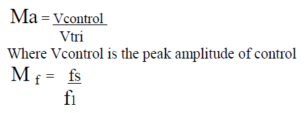
| The triangle waveform, vtri, is at switching frequency fs; this frequency controls the speed at which the inverter switches are turned off and on. The control signal, vcontrol, is used to modulate the switch duty ratio and has a frequency f1. This is the fundamental frequency of the inverter voltage output. Since the output of the inverter is affected by the switching frequency it will contain harmonics at the switching frequency. The duty cycle of the one of the inverter switches is called the amplitude modulation ratio, ma. |
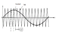 |
| Fig. 2 – Desired frequency is compared with a triangular waveform |
 |
| Fig. 3 – Pulse-width Modulation (PWM) |
 |
 |
| In fig. 3 the switches Ta+ and Ta- are controlled based on the comparison of vcontrol and Vtri (See equation 3). The two switches are never off at the same time which results in the output voltage fluctuating between +/- Vd/2.[1],[7],[13]. |
SPWM Switching Techniques |
| A. PWM with bipolar voltage switching |
| B. PWM with unipolar voltage switching |
A.SPWM with Bipolar Switching: |
| The basic idea to produce PWM Bipolar voltage switching signal is shown in Fig. 4 . It comprises of a comparator used to compare between the reference voltage waveform Vr with the triangular carrier signal Vc and produces the bipolar switching signal. If this scheme is applied to the full bridge single phase inverter as shown in Fig., all the switch S11, S21, S12 and S22 are turned on and off at the same time. The output of leg A is equal and opposite to the output of leg B.[3] |
| The output voltage is determined by comparing the reference signal, Vr and the triangular carrier signal, Vc. |
 |
| Fig.4 Bipolar PWM generator |
| In this scheme the diagonally opposite transistors S 11, S21, and S12 , S22 are turned on or turned off at the same time. The output of leg A is equal and opposite to the output of leg B. The output voltage is determined by comparing the control signal, Vr and the triangular signal, Vc as shown in Fig. 5 to get the switching pulses for the devices, and the switching pattern and output waveformis as follows.[2],[8]. |
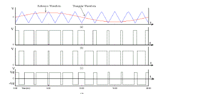 |
| Fig. 5: SPWM with Bipolar voltage switching (a) Comparison between reference waveform and triangular waveform (b) Gating pulses for S1 and S4 (c) Gating pulses for S2 and S3 (d) Output waveform |
 |
B. SPWM with Unipolar Switching: |
| In this scheme, the triangular carrier waveform is compared with two reference signals which are positive and negative signal. The basic idea to produce SPWM with unipolar voltage switching is shown in Fig. 6. The different between the Bipolar SPWM generators is that the generator uses another comparator to compare between the inverse reference waveform−Vr . The process of comparing these two signals to produce the unipolar voltage switching signal. The switching pattern and output waveform is as follows in Fig. 7. In Unipolar voltage switching the output voltage switches between 0 and Vdc, or switching event is halved in the unipolar case from 2Vdc to Vdc. The effective switching frequency is seen by the load is doubled and the voltage pulse amplitude is halved. Due to this, the harmonic content of the output voltage waveform is reduced compared to Bipolar switching. In Unipolar voltage switching scheme also, the amplitude of the significant harmonics and its sidebands is much lower for all modulation indexes thus making filtering easier, and with its size being significantly smaller. Between 0 and −Vdc. This is in contrast to the bipolar switching strategy in which the output swings between Vdc and −Vdc. As a result, the change in output voltage at each.[2], [6],[8] |
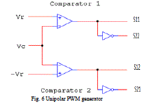 |
| Fig. 6 Unipolar PWM generator |
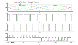 |
| Fig. 7 Waveform for SPWM with Unipolar voltage switching (a) Comparison between reference waveform and triangular waveform (b) Gating pulses for S1 and S4 (c) Gating pulses for S2 and S3 (d) Output waveform |
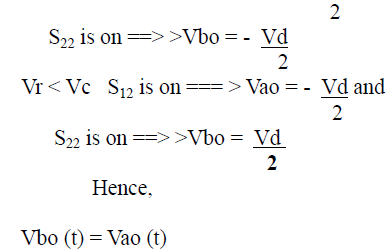
| In this scheme, the devices in one leg are turned on or off based on the comparison of the modulation signal Vr with a high frequency triangular wave. The devices in the other leg are turned on or off by the comparison of the modulation signal – Vr with the same high frequency triangular wave.[2],[8]. |
| The logic behind the switching of the devices in the leg connected to ‘a’ is given as, |
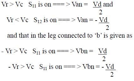 |
| In Unipolar switching scheme the output voltage level changes between either 0 to –Vd or from 0 to +Vd. This scheme ‘effectively’ has the effect of doubling the switching frequency as far as the output harmonics are concerned, compared to the bipolar- switching scheme[1],[2],[,3],[12],. |
Results |
| Here we design and test Unipolar Voltage Switching and also simulate in matlab.and see the switching pulses of both. |
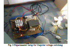 |
| Fig. 8 Experimental Setup for Unipolar voltage switching |
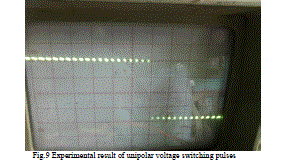 |
| Fig.9 Experimental result of unipolar voltage switching pulses |
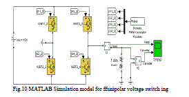 |
| Fig.10 MATLAB Simulation model for ffunipolar voltage switch ing |
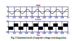 |
| Fig.11Simulated result of unipolar voltage switching pulses |
 |
CONCLUSION |
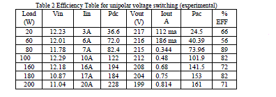
| In this paper the single phase SPWM microcontroller-based 300VA inverter is designed and tested for fixed modulation index 0.6 and unipolar voltage switching. It gives a different result of currents and voltages for different resistive loads. It was found that it gives maximum efficiency for 80W load upto 89%.and simulate this unipolar switching model in MATLAB. In order to accomplish a much better performance, several improvements (like change modulation index) are being made and the work is in progress. |
References |
|