International Journal of Advanced Research in Electrical, Electronics and Instrumentation Engineering
ISSN ONLINE(2278-8875) PRINT (2320-3765)
ISSN ONLINE(2278-8875) PRINT (2320-3765)
| ArunKumar.M1, Gowdra Vinay Kumar 2, Dr. Sanjay Lakshminarayanan3 |
| Related article at Pubmed, Scholar Google |
Visit for more related articles at International Journal of Advanced Research in Electrical, Electronics and Instrumentation Engineering
In this paper, FPGA based gate triggering pulses for five-level Cascaded Multilevel Inverter is designed. CORDIC algorithm is implemented on FPGA which is used for calculating different sine values. These sine values are used for generating gate pulses of five-level cascaded multilevel inverter. MATLAB/SIMULINK software was used for simulation and verification of proposed method.Gating signals are generated using FPGA Spartan-2 processor. The processor is designed using Verilog HDL using a structured coding method, simulated using Model Sim simulator and implemented using Xilinx 7.3FPGA synthesis Tool. The gating pulses are analysed and verified ,and compared with the actual pulses obtained from MATLAB/SIMULINK.
Keywords |
| Cascaded multilevel inverter, CORDIC,Verilog, MATLAB/SIMULINK, Gating pulses. |
INTRODUCTION |
| Multilevel inverter is used in applications that need high voltage and high current. The topologies of multilevel inverter have several advantages such as lower THD, lower EMI generation, better output waveform and higher efficiency for a given quality of output waveform. The elementary concept of a multilevel converter to achieve higher power is to use a series of power semiconductor switches with several lower voltage dc sources to perform the power conversion by synthesizing a staircase voltage waveform that approximates sine wave. Even though multilevel inverter has many advantages, one major disadvantage is the greater number of power semiconductor switches needed. This need of many power semiconductors switches results in complex control algorithm and switching strategy. Conventionally control algorithm and switching strategy is implemented on microprocessor or DSP processors. This type of processor executes the instruction sequentially; inherently they are slow and have low memory bandwidth. Field-programmable gate arrays (FPGAs) overcome above disadvantages, also the inherent parallelism of the logic resources on an FPGA allows for considerable computational throughput even at a low MHz clock rate. Due to these advantages FPGAs are well suited for multilevel inverter [1]. |
| The implementation of these complex algorithms requires computation of mathematical functions such as sine, cosineorsquareroots. These functions are computed using linear interpolation or power series techniques. While implementing on FPGAs usually the values are pre-computed and stored in lookup table (LUT) and if computation required by using interpolation or power series methods multipliers are used. LUTsarethefastestwaytomakethecomputation;buttheprecisionofthe resultis directly relatedtosizeof thelook-uptable. Theuseof powerseriesisslowtoconvergetoadesiredprecision and takes more iterations and depends on the availability of multipliers. One of the technique for calculating mathematical functions such as sine, cosine etc is for Co-ordinate Rotation Digital Computer (CORDIC) [3], [4]. Thismethod isacompromisebetween thetwomethods describedabovewhereintheprecisionispreservedwithoutany considerablememoryrequirement. |
| In this paper, a methodology for generating gating pulse for a multilevel inverter based on the cascaded multilevel inverter topology with equal dc sources is proposed. The main objective of this paper is it discusses about the gating pulse generation scheme for cascaded multilevel inverter. For generating gating pulses requires sine values at different instants of time. To compute the sine values CORDIC algorithm is used. This computed sine values is then used for computing gating pulses for cascaded multilevel inverter. |
| This paper organized as follows. Section – II discusses the working principle of cascaded multilevel inverter. Section – III describes the CORDIC algorithm method. Section – IV discusses about gating pulse generation method for cascaded multilevel inverter and simulation results. The proposed CORDIC algorithm method along with ModelSim simulation results are presented in section-V. Finally conclusions are summarized in section VI. |
II. OPERATION OF FIVE – LEVEL CASCADED MULTILVEL INVERTER |
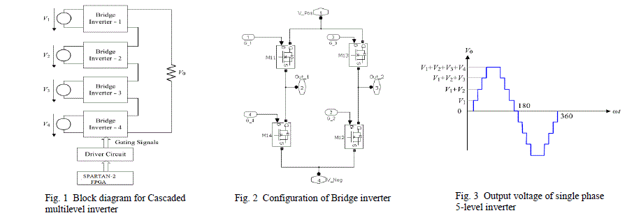
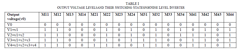
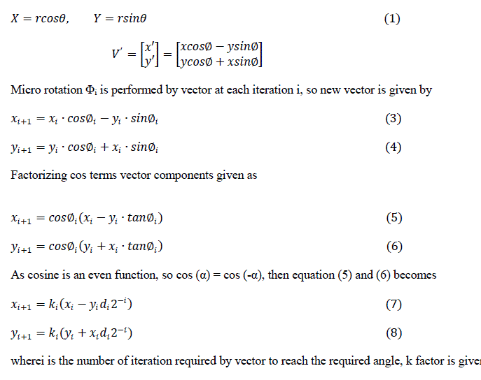
| A five – level cascaded type multilevel inverter is considered for this work. In this configuration, four single phase Hbridges are serially connected for nine – levelinverter. This results in a 5-levels of voltage in the positive half cycle and 5-levels of voltage in the negative half cycle including âÃâ¬Ãâ0‘ voltage level. In general the number of bridges required for an m level inverter is (m−1)/2. The block diagram of single phase cascaded five level inverter is shown in Fig. 1. Each bridge module comprisesof four Metal Oxide Semi-Conductor Field Effect Transistors (MOSFET) is shown in Fig. 2. Each bridge is energized by separateSources. Thus for nine – level inverter four DC sources are needed. The general function of this multilevel inverter is to synthesize a staircase voltage waveform that approximates sine wave as shown in Fig. 3 from several separate DC sources which may be obtained from batteries, fuel cells, solar cells or ultra – capacitors [2]. whereMij is the switches in the individual bridge,i is the number of bridge and j switch number in the inverter.Table I shows the voltage levels and their corresponding switch states in one quarter cycle of output voltage.State condition 1 means the switch is on and 0 means the switch is off. Each switch is turned on only once per cycleand therefore reduces switching losses. |
 |
 |
| The maximum output phase voltage is given as V0 = V1 +V2 + V3 + V4 as seen in Fig. 3.The steps to synthesize the nine -level voltage waveformsare as follows. |
| 1. For an output voltage level V0 = 0, no switch in the H-bridges are turned on. |
| 2. For an output voltage level V0 = V1, turn on the switches M11, M12, M22, M24, M32, M34, M42, M44. |
| 3. For an output voltage level V0 = V1 + V2, turn on all the switches as mentioned in step 2 and M41. |
| 4. For an output voltage level V0 = V1 + V2 + V3, turn on all the switches in the step 3 and M31. |
| 5. For an output voltage level V0 = V1 + V2 + V3 + V4, turn on all the switches in the step 3 and M21. |
III. CORDICALGORITHM |
| CORDIC is known as an iterative algorithm using only shift-and-add operations to perform several mathematic functions for scientific and engineering fields. CORDIC was firstly described in 1959 by J.E.Volder [3]to evaluate trigonometric functions. In 1971, J. Walther[4] extendedtheCORDICalgorithm tohyperbolicfunctionsandthealgorithm istodayusedin manyapplicationareassuchasmatrixcomputation,digital signalprocessing,digitalimageprocessing,communication,roboticsandgraphics. |
| CORDIC operates in two modes for computation of different functions, they are |
| ïÃÆÃË Rotation mode |
| ïÃÆÃË Vector mode |
| ïÃÂö Rotation mode: |
| In rotation mode, the co-ordinate components of a vector and an angle of rotation is given and the coordinate component of original vector, after rotation through given angle are computed. |
| ïÃÂö Vector mode: |
| In vector mode, the co-ordinate component of a given vector is given and the magnitude and angular arguments of original vector are compared. |
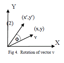
| The basic idea of CORDIC is to rotate the vector over given angle. Each basic rotation is realizedby using shift and add operation. A vector is rotated through fixed number of steps called asiterations. If a vector v as shown in Fig 4. having co-ordinates (x and y) is rotated through an angle Φ then obtaininga new vector with co-ordinates where x’ and y’ can be obtained using following method. |
  |
 |
|
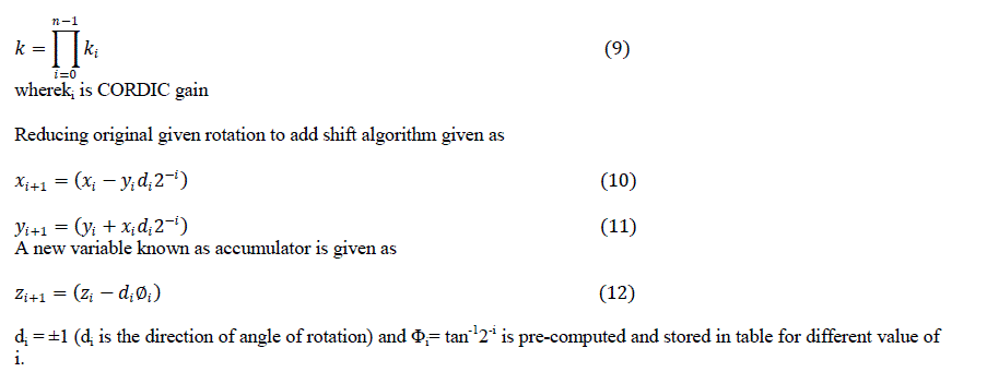
| Table II gives the computation for 300. |
 |
IV.CASCADED MULTILEVEL INVERTER GATING PULSES GENERATION SCHEME |
| The Simulink model of gate pulse generation scheme for cascaded multilevel inverter (CMLI) is shown in Fig. 5. The output of the Simulink model is shown in Fig. 6. As seen from the scheme sinusoidal signal is compared with different dc levels. Peak value of sinusoidal signal value is assumed as 1. In case of two level CMLI the dc levels compared are +0.5 and -0.5 as shown in Fig.5 (constant1 and constant2). First the sine signal separated into two parts one part consist of positive half cycle and the other part consists of negative half cycle. This is done by comparing the sine signal with constant value of 0.1 and -0.1 (this value is taken to avoid shoot through fault). Thus obtained signal is the gating signals for MOSFETs of bridge inverter-1 of Fig. 1 and this signal is named as G11G12 and G13G14 as seen in Fig. 6. If the compared sine signal lies between levels 0.1and 0.5 the obtained signal is then added with signals G11G12 and G13G14 respectively to obtain the gating signals G22 and G24 as shown in Fig. 6. |
 |
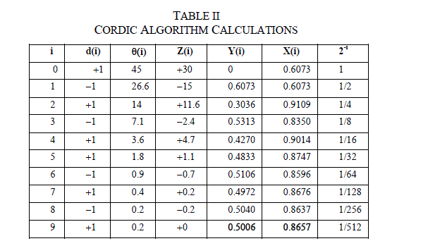
| In case nine level CMLI the number of constants levels is three and the levels are divided as 0.25, 0.5 and 0.75 and the same scheme as discussed above is extrapolated for five level CMLI and the following gating pulses shown in Fig. 7 is obtained. |
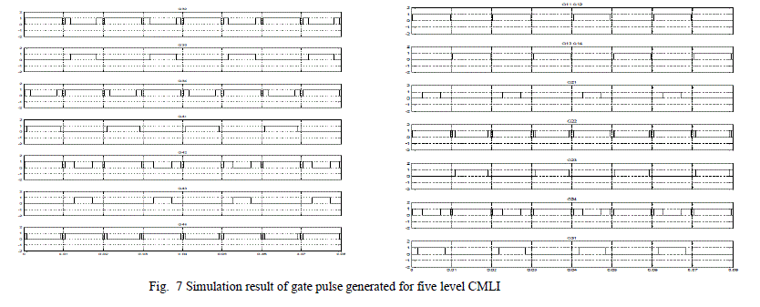 |
| The above gating pulse is applied to gates of MOSFETs of nine level CMLI as shown in Fig. 8 and simulated result of nine level CMLI output voltage waveform is shown in Fig. 9. |
 |
V. FPGA IMPLEMENTATION ANDRESULTS |
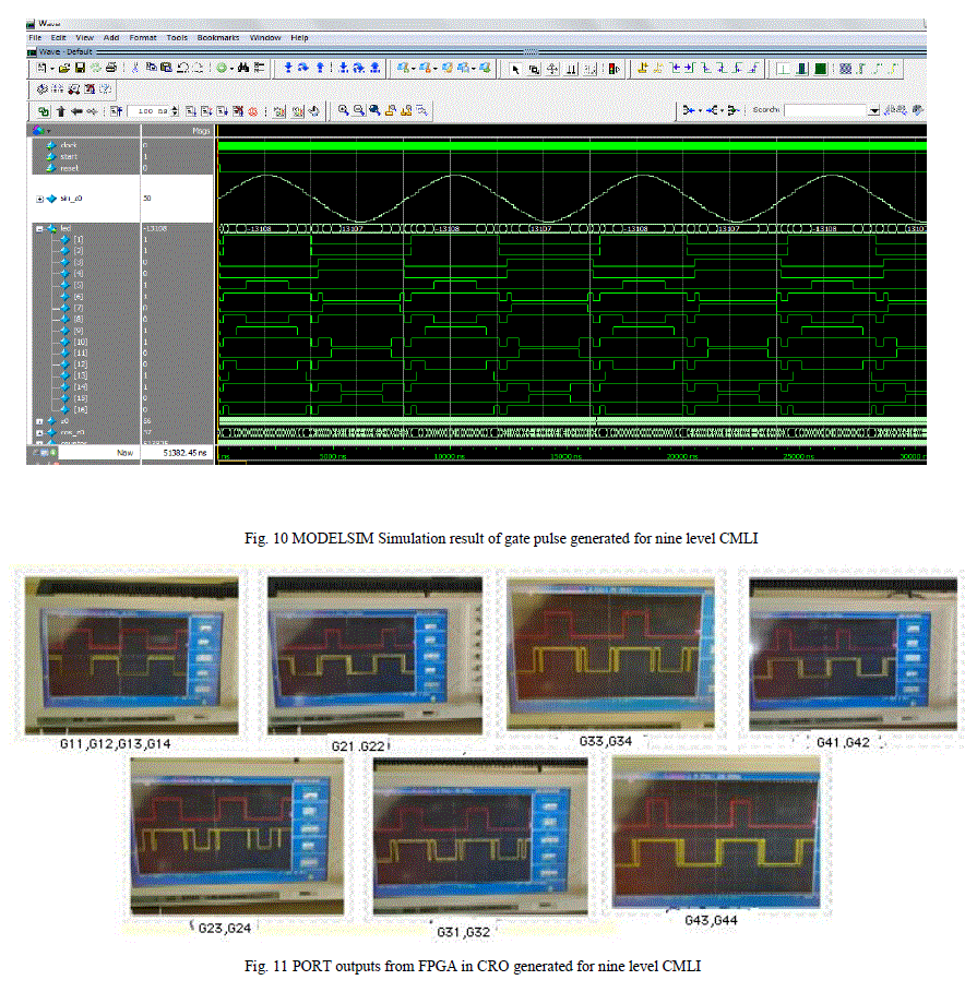
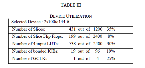
| The gating signal generation scheme as discussed in section III consists of comparing sinusoidal signal with different constant levels. In case of nine level CMLI the levels are 0.25, 0.5 and 0.75 respectively. In conventional method this is done by comparing sine wave with different dc levels and this is accomplished by comparator circuits. In this paper digital implementation is considered by using FPGA. The required sine values are computed as discussed in section II and gating pulses are generated as per the scheme discussed in section III. The family of FPGA device used is Spartan – 2 and the target device is xc2s100 having a clock speed of 4MHz. The programming language used is VERILOG and simulated using MODELSIM. Fig. 10 shown MODELSIM simulated result of gating pulse generated for nine level CMLI. Fig. 11 shows the port pin outputs of the FPGA and captured in the CRO. As seen in Fig. 11 the final output of the FPGA as in the CRO matches with the simulated results of MATLAB as seen in Fig. 7. This gating pulse thus generated is applied to nine level CMLI through driver circuit as shown in Fig. 1 to obtain the load voltage waveform as shown in Fig. 9. Table 2 gives the device utilization of the FPGA target device xc2s100 and it is observed that, the utilization of device is very economical. |
 |
 |
VI. CONCLUSIONS |
| A CORDIC based gate pulse generation scheme for nine level CMLI is discussed. CORDIC is a versatile algorithm and is used in application such as digital signalprocessing,digitalimageprocessing,communication,roboticsandgraphics. In this paper CORDIC algorithm is successfully implemented for gating pulse generation for CMLI. The most important feature is that look up table is not used for storing the sine values instead sine values are computed at the required instants of time. The main advantage of this method is that the accuracy of sine values thus computed is high which can give better performance with respect to EMI point of view. This method also gives better device utilization as seen in table III since CORDIC uses only shifters and adders instead of multipliers. |
References |
|