ISSN ONLINE(2319-8753)PRINT(2347-6710)
ISSN ONLINE(2319-8753)PRINT(2347-6710)
Jaspreet Kaur1, Gaurav Mittal2
|
| Related article at Pubmed, Scholar Google |
Visit for more related articles at International Journal of Innovative Research in Science, Engineering and Technology
Interpolation filters are integral part of a modern communication transmitter. This paper presents the design and FPGA implementation for a digital up converter or interpolation filter for a WiMAX Communication system. Multistage implementation approach has been used to reduce the hardware requirement. The results have been presented for a xc3sd1800a-4fg676 FPGA device.
Keywords |
| Digital Up Converter, FPGA, Interpolation, Multistage, WiMAX. |
INTRODUCTION |
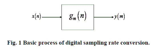
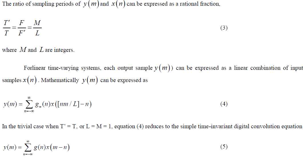
| Modern signal processing problems are often solved in the digital domain due to the availability of powerful VLSI circuits which allow to perform complex operations in real-time, without the well-known shortcomings of analog implementations. The source signal is transformed into the digital domain by an A/D converter. All data processing, e.g. filtering, shaping, mixing etc., is done in the digital domain and only the final result is converted back to analog. To overcome the degradation caused by successive A/D-D/A conversion, all processing blocks must have digital interfaces. Depending on the available bandwidth of the channel, the required quality, and the data rate of the interfaces a wide variety of sample rates are used. The incorporation of all these systems is however trouble-free, if a sample-rate converter is used at each interface. Samplerate conversion is used in the field of communications systems, speech processing systems, antenna systems and radar systems etc. Many types of sampling have been discussed in the literature including non-uniform sampling, uniform sampling, and multiple function uniform sampling. The most common form of sampling is periodic sampling in which |
 |
| i.e., the samples D x n are uniformly spaced in the dimension t , occurring nT apart. For uniform sampling we define the sampling period as T and the sampling rate as |
 |
 |
 |
 |
SAMPLING RATE UP CONVERSION |
| integer factor L, then the new sampling If the sampling rate is increased by an period T is |
 |
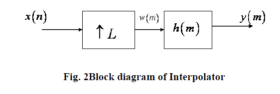
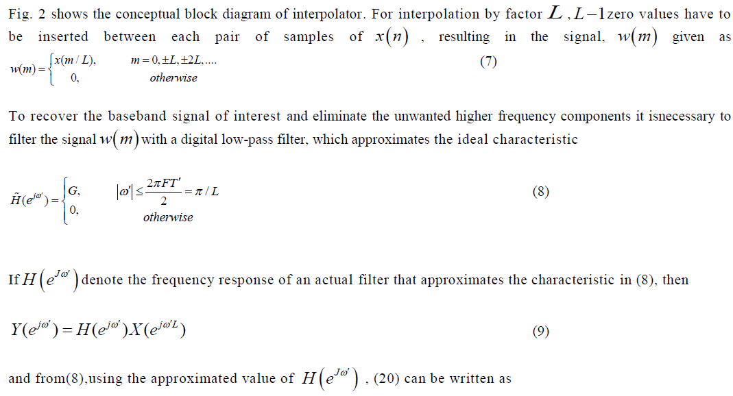
| and the new sampling rate F& LF . This process of increasing the sampling rate of a signal x(n) by L implies that we must interpolate L-1new sample values between each pair of sample values of x(n) . |
 |
 |
 |
DESIGN OF INTERPOLATION FILTER |
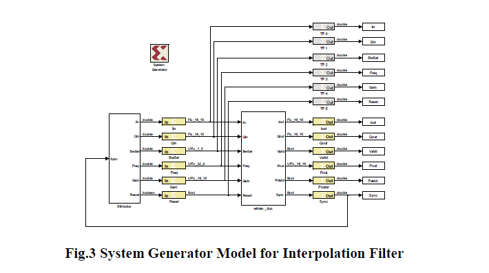 |
| Figure 3 show the complete setup developed using system generator and Figure 6 shows the details of DUC module. Figure 4 shows the internal view of multistage implementation of interpolation filterThe setup shown in Figure 3 has been simulated and synthesized using ISE 9.2i software. Table 1 shows the resources used by the design for xc3sd1800a-4fg676 FPGA device. |
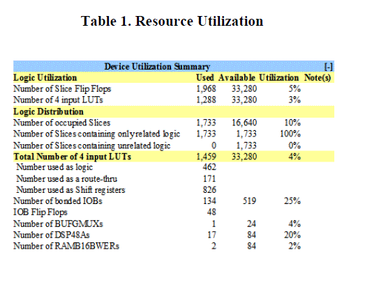 |
| From Table 1, it has been concluded that the proposed design uses only very small number of FPGA resources. |
CONCLUSION |
| DUC is in integral part of a digital communication receiver and its multistage design leads to the requirement of less number of FPGA resources. This paper shows the successful implementation of DUC for a WiMAX system. The resources utilized by the proposed design are well below the hardware utilization reported in previous works. |
References |
|