International Journal of Advanced Research in Electrical, Electronics and Instrumentation Engineering
ISSN ONLINE(2278-8875) PRINT (2320-3765)
ISSN ONLINE(2278-8875) PRINT (2320-3765)
| Indu.M1, Arun Kumar.M2 |
| Related article at Pubmed, Scholar Google |
Visit for more related articles at International Journal of Advanced Research in Electrical, Electronics and Instrumentation Engineering
This paper presents the design and implementation of a low power pipelined 32-bit RISC Processor. The various blocks include the Fetch, Decode, Execute and Memory Read / Write Back to implement 4 stage pipelining. In this paper, low power technique is proposed in front end process. Modified Harvard Architecture is used which has distinct program memory space and data memory space. Low power consumption helps to reduce the heat dissipation, lengthen battery life and increase device reliability. To minimize the power of RISC Core, clock gating technique is used which is an efficient low power technique. Verilog Language is used for coding purpose.7-SEG LEDs are connected to the RISC IO interface for testing purpose of all the instructions defined that is floating point numbers as well as integer values.The proposed architecture is then simulated using Modelsim. Dynamic power consumption is calculated using Altera powerplay analyser and then implementation is done using Altera Quartus II on Altera FPGA board.
Keywords |
| FPGA, RISC, Low Power, Clock Gating, Verilog, High Performance, Auto Branch Prediction |
INTRODUCTION |
| Low power has emerged as a principle theme in today’s electronics industry. The need for low power has caused a major paradigm shift where power dissipation has become an important consideration as performance and area. RISC is termed as Reduced Instruction Set Computer, computer arithmetic-logic unit that uses a minimal instruction set, emphasizing the instructions used most often and optimizing them for the fastest possible execution. This processor will follow the RISC architecture because it supports a predefined set of instructions. In this all the instructions have same length. Software for RISC processors must handle more operations than traditional CISC [Complex Instruction Set Computer] processors, but RISC processors have advantages in applications that benefit from faster instruction execution [1]. RISC processor design emphasizes on load/store architecture. The operations performed on chip registers are much faster than on memory due to the difference in the time taken to access the registers as well as memory. The access to memory is done only through load and store instructions. Due to faster execution, the operations are performed on the data present in the registers. They are also less costly to design, test, and manufacture [6]. |
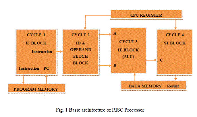
| The basic architecture of RISC Pipeline Processor is shown in fig 1 [4],[5]. |
 |
II. PROPOSED SYSTEM |
| The RISC Processor is designed using pipelined architecture. In this 4-stage pipelining is implemented, with this the speed as well as performance is increased. The four stages of pipeline are fetch, decode, execute and memory read/write back[1][6].During the design process, low power technique is included. For increasing the performance, latch based clock gating is used. Clock gating is most popular method used for reducing dynamic power consumption of clock signals. Power is mainly consumed by Combinatorial logic whose values are changing on each clock edge, flip-flops and by clock buffer tree in design. When the clock signal is not required to a particular module for some period, gating logic comes into picture to turn off the clock. Clock gating saves the power by reducing unnecessary switching activities. Gating logic is added in to the design by Integrated clock gating method(inserted into the design manually by the RTL designer)[2]. |
| Processors with pipelining consists of modules internally which can work on microinstructions separately. Each stage in the pipeline is linked to next stage by flip-flops, through this the overall processing time is reduced as output of previous stage acts as an input to next stage. An instruction pipeline is said to be fully pipelined if it accept a new instruction every clock cycle. |
| The proposed processor is 32 bit low power RISC processor with pipelining architecture which gets instructions on a regular basis using dedicated buses to its memory, executes all its native instructions in stages with pipelining. It can communicate with external devices with its dedicated parallel IO interface |
A. Types of Instructions |
| There are basically three types of instructions namely Arithmetic and Logical Instructions (ALU instructions), Load/Store instructions and Branch instructions[1] |
1. ALU Instructions: |
| Arithmetic operations either take two registers as operands or take one register and a sign extended immediate value as an operand. Some arithmetic instructions are addition, subtraction, multiplication, division, increment, decrement. The result is stored in a third register. Logical operations such as and ,or, xor do not usually differentiate between 32-bit and 64-bit. Other logical instructions are nand, nor, not, xnor, right shift, left shift etc. |
| 2. Load/Store Instructions: |
| By taking a register (base register) as an operand and a 16-bit immediate value and the sum of the two will create the effective address. A second register acts as a source in the case of a load operation. In the case of a store operation, the second register contains the data to be stored. |
3. Branches and Jumps: |
| Conditional branches are transfers of control. A branch causes an immediate value to be added to the current program counter. Some common branch instructions are BZ (Branch Zero), BRC (Branch if Carry), JMP (Jump Instruction), JMPZ (Jump when zero), Cmp(compare two operands and based on this carry flag is updated with one or zero) etc. |
III. ARCHITECTURE |
| The Proposed architecture consists of |
| ïÃâ÷ Instruction Fetch(IF) |
| ïÃâ÷ Instruction Decode(ID) |
| ïÃâ÷ Execution unit(EX) |
| ïÃâ÷ Memory unit(MU) |
| ïÃâ÷ Memory read/write unit |
| ïÃâ÷ Low Power unit |
| ïÃâ÷ Four general purpose registers namely register R0, register R1, register R2 and register R3 |
| ïÃâ÷ Floating point unit |
 |
| B. Instruction Fetch |
| This stage consists of Program counter, Instruction Memory, and the Branch Decide unit. |
| 1. Program Counter: |
| The program counter (PC) contains the address of the instruction that will be fetched from the Instruction memory during the next clock cycle. Normally, the PC is incremented by one during each clock cycle unless a branch instruction is executed. When a branch instruction is encountered, the PC is incremented by the amount indicated by the branch offset. |
| 2. Instruction Memory: |
| The Instruction Memory contains the instructions that are executed by the processor. The input to this unit is a 9-bit address from the program counter and the output is 9-bit instruction word. |
| 3. Branch Decide Unit: |
| The Branch Decide Unit is responsible for determining whether a branch is to take place or not based on the 2-bit Branch signal from the control Unit and the Zero flag from the Arithmetic and Logic Unit (ALU). |
| B. Instruction Decode |
| This stage consists of the Control Unit, Register File. |
| 1. Control Unit: |
| The control unit generates all the control signals needed to control the coordination among the entire component of the processor. This unit generates signals that control all the read and write operation of the register file, and the Data memory. It is also responsible for generating signals that decide when to use the multiplier and when to use the ALU, and it also generates appropriate branch flags that are used by the Branch Decide unit. |
| 2. Register file: |
| This is a two port register file which can perform two simultaneous read and one write operation. It contains four 32-bit general purpose registers. The registers are named R0 through R4 |
| C. Execute |
| This stage consists of the Branch Adder, Arithmetic Logic Unit (ALU), and the ALU Control Unit. |
| 1. Branch Adder: |
| The branch adder adds the 26-bit signed branch offset with the current value of the PC to calculate the branch target. The 26-bit offset is provided by the branch instruction. The output of this unit goes to the PC control multiplexer which updates the PC with this value only when a branch is to be taken. |
| 2. Arithmetic Logic Unit (ALU): |
| The ALU is responsible for all arithmetic and logic operations that take place within the processor. These operations can have one operand or two, with these values coming from either the register file or from the immediate value from the instruction directly. All operations are done according to the control signal coming from ALU control unit |
| 3. ALU Control Unit: |
| This unit is responsible for providing signals to the ALU that indicates the operation that the ALU will perform. The input to this unit is the 5-bit opcode and the 2-bit function field of the instruction word. It uses these bits to decide the correct ALU operation for the current instruction cycle. This unit also provides another set of output that is used to gate the signals to the parts of the ALU that it will not be using for the current operation. This stage consists of some control circuitry that forwards the appropriate data, generated by the ALU or read from the Data Memory, to the register files to be written into the designated register |
| D. Memory |
| This stage consists of the Data/Instruction Memory module |
| 1. Data/Instruction Memory: |
| The architecture used is Modified Harvard architecture. This module supports 512 depth of 32-bit data words. The Load and Store instructions are used to access this module. Finally, the Memory Access stage is where, if necessary, system memory is accessed for data. Also, if a write to data memory is required by the instruction it is done in this stage. In order to avoid additional complications it is assumed that a single read or write is accomplished within a single CPU clock cycle. |
| The architecture uses dynamic branch prediction as it reduces branch penalties under hardware control [1],[5]. The Prediction is made in Instruction Fetch stage of the pipeline. Thus branch prediction buffer is indexed by the lower order bits of the branch address in Instruction Fetch. It is low for branch not taken and high for branch taken and branch target can be accessed as soon as the branch target address is computed. Branch Target cache is a branch prediction buffer with addition information as it has an address tag of a branch instruction and stores the target address. Thus BTC determines if the instruction is a branch and, if branch will be taken and, if branch prediction is taken, and what will be the target address. If these requirements are met the processor can initiate the next instruction access as soon as the previous access is complete. Thus the main operation of BTC is that during the IF stage, the lsbs of the PC are used to access the BTC and if the msbs of the PC match the target then the entry is valid. If the branch is predicted as taken, the predicted target address is used to access the I-cache during the next cycle. |
| 2. Modified Harvard architecture: |
| The Modified Harvard architecture is a variation of the Harvard computer architecture that allows the contents of the instruction memory to be accessed as if it is data .Most modern computers that are documented as Harvard architecture are, in fact, Modified Harvard architecture. The modifications are to loosen the strict separation between code and data, while still supporting the higher performance concurrent data and instruction access of the Harvard architecture [1]. |
| The most common modification builds a memory hierarchy with a CPU cache separating instruction and data. This unifies all except small portions of the data and instruction address spaces, providing the Von Neumann model. The programmers never need to be aware of the fact that the processor core implements a (modified) Harvard architecture, although they benefit from its speed advantages. Only programmers who write instructions into data memory need to be aware of issues such as cache coherency and executable space protection. |
| E. Low power unit |
| The power reducing technique that has been explored in this architecture is clock gating. Clock gating is a method which prevents the clock signal reaching the various modules when there is no demand. The non availability of clock signal prevents the register or flip-flops from changing their states. As a result the input to any combinational circuit remains unchanged and thus no switching activity takes place. Most of the power dissipation results from switching activity, clock gating greatly reduces the power consumption [7],[10]. |
| F. Floating point unit |
| Floating point is the most common representation of real numbers on computers. Floating-point employs a sort of "sliding window" of precision appropriate to the scale of the number. This allows it to represent numbers from 1,000,000,000,000 to 0.0000000000000001 with ease [3]. |
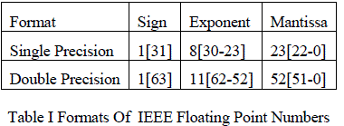
| 1. Formats: |
| IEEE floating point number have three basic components: the sign, the exponent, and the mantissa. The mantissa is composed of the fraction and an implicit leading digit. The exponent base (2) is implicit and need not be stored. There are two basic number formats in IEE754, single precision, and double precision. In this paper single precision format is used. The number of bits for each field are shown (bit ranges are in square brackets): |
 |
| 2. General format: |
| (±1)S × (1+F) × 2E |
| Where |
| ïÃâ÷ S = sign, 0 for positive, 1 for negative |
| ïÃâ÷ F = fraction (or mantissa) as a binary integer,1+F is called significand |
| ïÃâ÷ E = exponent as a binary integer, positive or negative (two’s complement) |
| 3. Exceptions: |
| The IEEE standard defines five types of exceptions that should be signalled through a one bit status flag when encountered[3].In this paper we are concentrating only on four of them. |
| ïÃâ÷ Invalid Operation |
| Some arithmetic operations are invalid, such as a division by zero or square root of a negative number. The result of an invalid operation shall be a NaN (Not a number). There are two types of NaN, quiet NaN (QNaN) and signaling NaN (SNaN). They have the following format, where s is the sign bit: |
| QNaN = s 11111111 10000000000000000000000 |
| SNaN = s 11111111 00000000000000000000001 |
| The result of every invalid operation shall be a NaN string with a QNaN or SNaN exception. The following are some arithmetic operations which are invalid operations and that gives a result a QNaN string and that signal a QNaN exception: |
| ïÃâ÷ Any operation on a NaN |
| ïÃâ÷ Addition or subtraction: ∞ + (−∞) |
| ïÃâ÷ Multiplication: ± 0 × ± ∞ |
| ïÃâ÷ Division: ± 0/ ± 0 or ± ∞/ ± ∞ |
| ïÃâ÷ Square root: if the operand is less than zero |
| ïÃâ÷ Inexact |
| This exception should be signalled whenever the result of an arithmetic operation is not exact due to the restricted exponent and/or precision range. |
| ïÃâ÷ Underflow |
| Two events cause the underflow exception to be signalled, tininess and loss of accuracy. Tininess is detected after or before rounding when a result lies between ±2Emin. Loss of accuracy is detected when the result is simply inexact or only when a renormalizations loss occurs. The implementer has the choice to choose how these events are detected. They should be the same for all operations. The implemented FPU core signals an underflow exception whenever tininess is detected after rounding and at the same time the result is inexact |
| ïÃâ÷ Overflow |
| The overflow exception is signalled whenever the result exceeds the maximum value that can be represented due to the restricted exponent range. It is not signalled when one of the operands is infinity, because infinity arithmetic is always exact. Division by zero also doesn’t trigger this exception. |
| G. Instruction Set |
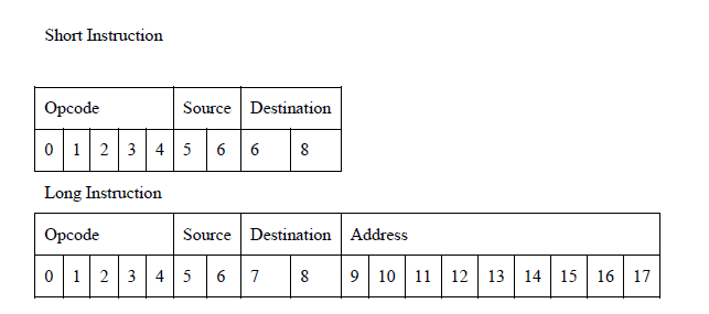
| The instruction set used in this architecture consists of arithmetic instructions, logical instructions, branch instructions and memory instructions. It will have short(9-bit) and long(18-bit) instructions. For all arithmetic and logical operations 9-bit instructions are used and for all memory and branch operations 18-bit instructions are used. It will have special instructions to access external ports. |
 |
| H. Addressing Modes Used |
| Addressing modes are aspects of the instruction set architecture in most central processing unit (CPU) designs [1]. The different addressing modes in a instruction set architecture define how machine language instructions in that architecture identify the operand (or operands) of each instruction. An addressing mode specifies how to calculate the effective memory address of an operand by using information held in registers and/or constants contained within a machine instruction or elsewhere. The various addressing modes used in proposed method are |
| ïÃâ÷ Direct addressing mode |
| ïÃâ÷ Immediate addressing mode |
| ïÃâ÷ PC-relative addressing mode (specifically for branch instruction) |
| ïÃâ÷ Register addressing mode |
| I. Features of proposed architecture |
| ïÃâ÷ It is 4- stage low power pipelining processor. |
| ïÃâ÷ It provides hazard detection unit to determine when stall must be added. |
| ïÃâ÷ Each functional unit can only be used once per instruction. |
| ïÃâ÷ Each functional unit has to be used at the same stage as all other instructions. |
| ïÃâ÷ Pipeline Control: that is each stage control signal depends only on the instruction that is currently in that stage. |
| ïÃâ÷ It provides halt support. |
| ïÃâ÷ It is capable of providing high performance. |
| ïÃâ÷ Pipelining would not flush when branch instruction occurs as it is implemented using dynamic branch prediction. |
| ïÃâ÷ Take cares of order-of-execution |
IV. SIMULATION RESULTS |
| Modelsim is used for simulation and results have been verified. The complete project has been developed on FPGA, Altera development and education board 2 platform, which has different testing and debugging scopes such as push button switches, toggle switches, LCD and LEDs. So all the testing has been carried out on the board. 7-SEGMENT LEDs is connected to RISC IO Interface for testing purpose. Different ouput patterns have been generated with RISC instructions, and are outputted on 7-SEGMENT LEDs.In Altera family, in order to implement the design the “QUARTUS-II” has been chosen and in the family “CYCLONE II”, the package used is “EP2C35F672C6” on Altera DE2 board. |
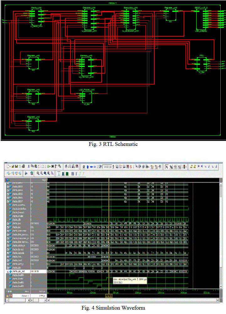
| The RTL schematic of the proposed method is shown in fig 3 |
 |
| A. Design Summary, Simulation and Synthesis result |
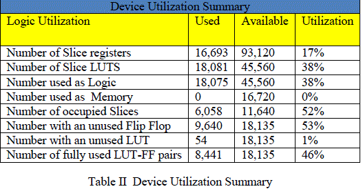
| 1. Design Summary: |
| The device utilisation summary is shown in table II which gives the detail of availability along with used number of resources in % using Xilinx ISE 13.1 web pack. |
 |
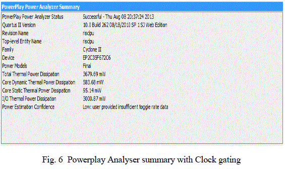
| 2. Power Analyser Summary: |
 |
 |
V. CONCLUSION |
| In this paper 4-stage Low Power Pipelined 32-bit RISC processor based on FPGA system is designed with Verilog coding adopted. Architecture is devised in order to felicitate the writing codes in Verilog. The Verilog coding synthesis issues play a vital role in speed –area optimality because RTL schematic depends heavily on coding flow in Verilog. The RISC Processor design is simulated and implemented on hardware and verified for its Arithmetic operations of both fixed and floating point numbers, Branch and Logical Functions. Arithmetic unit has been designed to perform four operations addition, subtraction, multiplication, and division on floating point numbers. IEEE 754 standard based floating point representation has been used. After synthesis we got the less no of logic resource utilization comparing the available resources which is shown in the device utilization summery table. Using the Altera Quartus II, the power consumed is calculated and comparision of dynamic power consumption with Clock gating and without Clock gating is done and the results has been shown in power analyser summary. |
ACKNOWLEDGMENT |
| This paper is dedicated to our family and parents for their endless support and encouragement. We would like to thank our friends for their constant support and guidance. We would like to thank the Department of Electronics and Communication Engineering, East Point College of Engineering and Technology, Bangalore for their constant support and encouragement in undertaking the work. |
References |
|