Keywords
|
| MCT, electrochemical photovoltaic detector, efficiency and fill factor |
INTRODUCTION
|
| The use of ternary semiconducting compounds as light absorbers in photon energy converters is an elegant technique to tailor the match between the electro-magnetic spectrum and the characteristic properties of the absorbers, especially when a sandwiched array of converters is considered, each being specialized for a part of the electro-magnetic spectrum. In aiming for the goal of fabricating such tandem devices we have been concerned with the synthesis of the ternary materials (II-IV-VI) in thin film form that are best contender due to their steep rise of the absorption coefficient at the threshold and direct mode of transitions. |
| The action spectra of these materials show a good deal of enhancement over a wide range of photon energies. Mercury- Cadmium-Telluride (MCT) is such a semiconductor material, which has shown a great promise as a material for electromagnetic radiation converters [1-2]. With this material, a relatively large fraction of the electromagnetic spectrum can be utilized and therefore, it is, reasonable to hope a considerable enhancement in the quantum conversion efficiency. This paper is a simplest attempt to synthesize the HgxCd1-xTe photosensitive material chemically and to employ it in an electrochemical photo-voltaic detector system. |
EXPERIMENTAL DETAILS
|
| HgxCd1-xTe (0 ≤ x ≤ 0.5) thin films of different compositions were obtained on the cleaned stainless steel and glass substrates using a simple chemical technique [2-6]. For the synthesis, A.R. grade solutions of cadmium chloride, mercuric chloride and refluxed sodium tellurosulphite were taken together and complexed with a sufficient quantity of Triethanolamine. pH of the resulting mixture was adjusted to 10 ± 0.2 and a predetermined quantity of liquid ammonia was added directly in to the reaction mixture to increase the film adherence. The cleaned substrates were then positioned on a substrate holder and kept rotating at 70 ± 2 r.p.m. speed in the reaction mixture, which was maintained at 80oC. The deposition was carried out for 90 min and then the samples were taken out of the reaction mixture, washed with double distilled water and preserved in dark. |
| An electrochemical photovoltaic detector was devised in an H-shaped glass cuvette using one of these electrode systems as a photosensitive electrode, sodium sulphide/polysulphide redox electrolyte and graphite rod as a counter electrode. The power output characteristics were obtained for all the detector configurations under a constant input light intensity of 20 mW/cm2 (tungsten filament lamp, 250W). A potentiometric arrangement in a two-electrode detector system was used for this purpose. |
| The generated photo potentials and photocurrents were noted for various incident intensities from 5 mW/cm2 to 35 mW/cm2. The spectral responses of the various detector systems were examined in the range of wavelengths from 400 nm to 1300 nm. The dynamic I–V and C–V characteristics in dark were obtained potentiometrically. A three- electrode detector system was used for the C-V measurements. A saturated calomel electrode (SCE) was used as a reference electrode. An Aplab-4910 LCR-Q meter was used to measure the junction capacitance whereas the I–V characteristics were obtained as usual. The reverse leakage current of these detectors was noted in the 373 to 300 K temperature ranges to calculate the built–in potentials Φβ. 6 ½ digit H.P. and 4 ½ digit HIL 2665 multimeters were used for the measurement of currents and voltages. Illumination intensities were recorded by a Lutron – 101 (Taiwan) luxmeter. A ten–turn 1 kΩ helical potentiometer was used to vary the junction potential. The surface morphology of these detector materials was observed through a scanning electron microscope, CAMECA SU-30 (France). The X-ray diffractograms were obtained for these electrode materials in the scanning range of 2θ from 20o to 80o. A Philips, PW-3710 X-ray diffractometer was used for this purpose. |
RESULTS AND DISCUSSION
|
| HgxCd1-xTe thin film photo electrodes of varying composition parameter x from 0 to 0.5 were deposited onto wellpolished stainless steel substrates by a simple chemical growth technique reported elsewhere [7-8]. The as-grown electrode materials were relatively uniform, mechanically hard, diffusely reflecting and tightly adherent to the substrate support with milky white in colour throughout the range studied. The composition dependent growth mechanism was studied and it has been observed that, the photoelectrode thickness decreased nonlinearly with the photoelectrode composition. Similar observations are available in the literature and can be explained as usual [3-6]. |
| The electrochemical photo-voltaic detector set in a glass cuvette with HgxCd1-xTe photo electrodes and sodium sulphide/polysulphide electrolyte illuminated by a light of photon energies greater than the optical gap of a semiconductor electrode. The excess charge carriers, which are generated as a result of the photon absorption, are separated at the space-charge region, the electrons move deep into the bulk, while holes arrive at the surface of the semiconductor that causes redox reactions in the electrode/electrolyte system. The charge separation process continues until it results in a counter field, which is maximized at the open circuit condition. |
| The current-voltage characteristics have been analyzed to yield the junction quality factor, nd from the linear region of the log Id versus V plots as shown in Figure 1. |
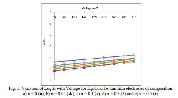 |
| The calculated values of nd are cited in the Table. |
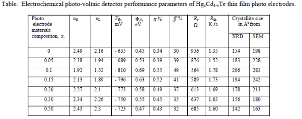 |
| It has been found from the magnitude of junction quality factors (nd) that recombination is the dominant mechanism at the interface. The junction quality factors (nd) has systematic variation, and as expected, it is smaller for x = 0.1, showing a less trap density at the interface formed by this photoelectrode. The semiconductor/electrolyte interface (electrochemical photovoltaic detector) can be modelled as a Schottky barrier and it is, therefore, possible to represent the current-voltage characteristic by the relation, |
 |
| where I is the net current density, Iph and Id are the photo and dark current densities, respectively. Io is the reverse saturation current density, V is the applied bias voltage and nd is the junction ideality factor. For bias voltages exceeding 3kT/q and in the equilibrium open- circuit conditions ( Iph = Id, V = Vph ), (1) can be rearranged as, |
 |
| where Vph is the maximum voltage at the open circuit condition and Iph is the short circuit current density. Under this condition, because Iph α FL, the incident light intensity and Iph >> Io, (2) reduces to, |
 |
| A plot of Vph versus ln Iph should therefore yield a straight line as shown in Figure 2. |
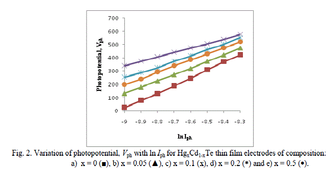 |
| The lighted quality factor nL of the junction may then be computed for these detector configurations and are cited in the Table. As the short circuit current is an approximately linear function of the light intensity, we have also studied the variations of Iph with FL for these electrochemical photovoltaic detectors. The linear dependence of the short circuit current also demonstrates that the transport of electro active species to the electrode / electrolyte interface does not limit the rate of the overall charge transfer reaction over the range of incident intensities employed [9-10]. |
| In a semiconductor / electrolyte system, the nature of charge transfer process across the interface is defined by a wellknown Butler-Volmer relation. The capacitance-voltage measurements were made on these photo-voltaic detector cells to evaluate the flat band potential, which determines the relative positions of the Fermi levels of semiconductor and an electrolyte and in turn the amount of band bending at the interface. The intrinsic band bending at the interface is a measure of the depletion layer width inside the semiconductor, and hence it determines the ability of the electrode to operate at the short circuit condition, which is also equivalent to a measure of the maximum open circuit voltage that can be achieved from the photo-voltaic detector. For a semiconductor / electrolyte interface, the space-charge capacitance is related to the applied voltage across it is, |
 |
| where Vfb is the flat band potential and other symbols have their usual meanings. The Mott-Schottky plots have been constructed to determine the actual values of the flat band potentials. The flat band potentials obtained by extrapolating the linear region of the C-2 versus V variations on the voltage-axis and the values are cited in the Table. It has been observed that the variation of Vfb with photoelectrode composition, x reached a maximum at x = 0.1. This change in Vfb with electrode composition could be ascribed to the decrease in the electron affinity as a result of the introduction of Hg into CdTe-lattice and an increased amount of surface adsorption [11-12]. The plots of log (Io/T2) versus 1000/T are shown in Figure 3. |
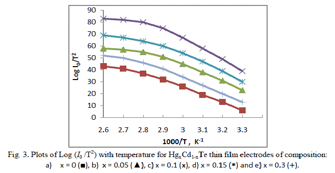 |
| The values of built-in potentials Φβ for these electrochemical photovoltaic detectors were determined from the linear regions of these plots. |
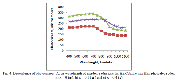
| These interfaces were further characterized through the power output characteristics under a constant illumination of 20 mW/cm2 and the photo potentials and photo currents as the functions of photoelectrode composition, x were plotted as usual. The variations in photocurrents with respect to the wavelength of incident radiations are shown in Figure 4. Typically, the quantum conversion efficiency η% and fill factor ff % have been enhanced from 0.24% to 0.55% and 30% to 49% respectively. The other performance parameters such as series resistance Rs, shunt resistance Rsh, response/switching time etc of these electrochemical photo-voltaic detectors were computed and their values are documented in the Table. It is clear that the overall performance of the electrochemical photovoltaic detector is improved significantly at x = 0.1 and can be interpreted from the following theoretical relation, |
 |
| where the symbols have their usual meanings. The maximum conversion efficiency ηmax depends on Vfb and Eg. In this case, the radiation detector delivered maximum power output at x = 0.1 and could be attributed to a larger value of the flat band potential shown by the detector. For the electrochemical photovoltaic detector with an n-type semiconductor photoelectrode, the larger the value of the flat band potential, more negative is the photoelectrode and greater is the possible output voltage. The enhancement in the flat band potential/open circuit photo potential is caused due to the creation of the new donor levels by substitution of Cd2+ ions by Hg2+ ions which effectively shift the Fermi level in the upward direction increasing the amount of band bending and hence the open circuit photo potential [12]. |
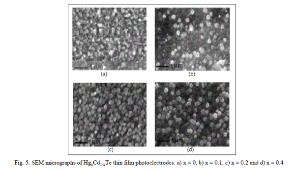 |
| The incremental changes in the photocurrent can be correlated to the modifications in the photoelectrode properties such as increased photoelectrode absorption, decreased band gap and series resistance of the detector material, improved crystallite size etc. as a result of introduction of Hg2+ in CdTe-lattice. The enhancement in both Vph and Iph could also be understood from the surface topographic observations and XRD analysis for this electrode material. |
| The XRD diffractograms of these as-deposited thin films of all compositions within the 2ïÃÂñ (20o-80o) ranges were studied and the composites revealed that they are polycrystalline in nature and the crystallite size went on increasing as electrode materials composition increased and there is a weak variation of lattice parameters. The average crystallite sizes were determined as usual both from XRD patterns and SEM micrographs (Figure 5) for all the compositions and are cited in the Table. It is observed that, there is a good agreement between crystallite sizes calculated from XRD patterns and SEM observations. The improved crystallite structure, decreased band gap, increased photo electrode absorption and electrical conductivity caused the series resistance Rs of a photo-voltaic detector to decrease resulting in the increased photocurrent and hence the quantum conversion efficiency. |
CONCLUSIONS
|
| The chemical bath deposition technique is found to be useful to synthesize HgxCd1-xTe thin film electrodes suitable for electrochemical photo-voltaic detection. An attempt is made to investigate the various electrochemical properties of an electrochemical photo-voltaic detector as a function of the photo electrode materials composition. The detector performance is found to be enhanced and became optimum at x = 0.1. The enhancement in the photopotential, Vph, is ascribed to the increased flat band potential, Vfb, increased photoelectrode absorption and improved crystallite structures. The increase in photocurrent, Iph, is mainly due to the decrease in the photoelectrode resistance and band gap of the material and increased absorption of the incident radiations by the photo sensitive electrode material. |
ACKNOWLEDGEMENTS
|
| Author is thankful to the authorities of Rayat Shikshan Sanstha, Satara and Hon. Prin. Dr. Arvind Burungale, Secretary, Rayat Shikshan Sanstha, Satara and Prin. Dr. V. S. Shivankar for their concern towards the research activity and quality consciousness. |
| |
References
|
- N. C. Sharma, D. K. Pandya and K. L. Chopra, “Electroless deposition of epitaxial Pb1-xHgxS films”, Thin Solid Films, vol. 59, no. 2, pp.157-164, May 1979.
- C. Levy-Clement, R. Triboulet and R. Tenne, “Photoelectrochemical properties of the Cd-rich CdxHg1-xTe alloy”, Solar Ener.Mater., vol. 17,no. 3, pp. 201-206, Apr-May 1988.
- L. P. Deshmukh and S. G. Holikatti, J. of Phys, D: Appl. Phys., “A CdS:Sbphotoelectrode for photoelectrochemical applications”, vol. 27, pp. 1786-1792, 1994.
- G. S. Shahane, B. M. More, C. B. Rotti and L. P. Deshmukh, “Studies on chemically deposited CdS1 - xSex mixed thin films”, Mat. Chem Phys., vol. 47, no. 2-3, pp. 263-267, Feb.1997.
- V. B. Pujari, V. B. Gaikwad, E. U. Masumdar, P. D. More and L. P. Deshmukh, “Chemically Synthesized (Cd, Hg) Se Pseudo-binaries: SomeCharacteristic Properties”, Turk. J. of Phys., vol. 26, no. 5, pp. 407-413, Sept. 2002.
- V. B. Pujari, S. H. Mane, V. S. Karande, J. S. Dargad and L. P. Deshmukh, “Mercury–cadmium–selenide thin film layers: structural,microscopic and spectral response studies”, Mat Chem. Phys., vol. 83, no. 1, pp. 10-15, Jan. 2004.
- S. H. Mane, V. S. Karande, V. B. Pujari and L. P. Deshmukh, “A study of cadmium mercury telluride (CMT) thin film structures: somephysical observations and characteristics”, J. of Mater. Sci.: Mater. in Elect, vol. 16, no. 11-12, pp. 733-739, Nov. 2005.
- C. Levy-Clement, R. Triboulet and R. Tenne, “Photoelectrochemical properties of the Cd-rich CdxHg1-xTe alloy”, Sol. Ener.Mater., vol. 17, no. 3, pp. 201-206, Apr-May 1988.
- K. Rajeshwar, P. Sing, R. C. Kainthla and K. L. Chopra, “Photoelectrochemical Characterization of CdSe Thin Film Anodes”, J. ofElectrochem. Soc., vol. 128, no. 8, pp. 1744-1750, 1981.
- V. B. Pujari and L. P. Deshmukh, “photoelectrochemical investigations on HgxCd1-xSe Thin Film Electrode/Electrolyte System”, Turk. J. ofPhys., vol. 32, no. 2, pp. 105-114, Mar 2008.
- P. K. Mahapatra and A. R. Dubey, Solar Ener. Mat. and Solar Cells, “Photoelectrochemicalbehaviour of mixed polycrystalline n-type CdSCdSeelectrodes”, vol. 32, no. 1, pp. 29-35, January 1994.
- R. N. Noufi, P. A. Kohl and A. J. Bard, “Semiconductor Electrodes XV.Photoelectrochemical Cells with Mixed Polycrystalline n-TypeCdS/CdSe Electrodes”, J. of Electrochem. Soc., vol. 125, no. 3, pp. 375-379, 1978.
|