Keywords
|
| Frequency response, capacitive voltage transformer, magnitude response, phase response |
INTRODUCTION
|
| In case of high voltage systems, the cost, design and manufacturing complexity of the conventional inductive voltage transformer is high due to more insulation requirement. Capacitive Voltage Transformers (CVTs) are extensively used to convert the line voltages of transmission and sub-transmission networks to low voltages which can be directly used as input to protection, measurement and control equipments in the system. The CVTs also meet the basic requirment of instrument transformers by providing electrical isolation and protection to the low voltage substation equipment from the high voltage lines[1,2,3]. The coupling capacitors of CVT can be used in Power Line Carrier(PLC) communication which is an uniuqe feature. |
| The secondary voltage of a CVT mirrors the scaled down primary voltage with predefined ratio during the steady state. The output signal of the CVTis no longer a replica of the primary voltage during the system transient conditions due to the presence of energy storage elements in the CVT. The distortion in the output singal of the CVT under system transient condition consists of various frequency components which last for short duration. This paper presents a review of the CVT frequency response with parametric varaition and explains the effect of various design parameters on the inaccuracies at non fundamental frequencies. |
CAPACITIVE VOLTAGE TRANSFORMER MODEL
|
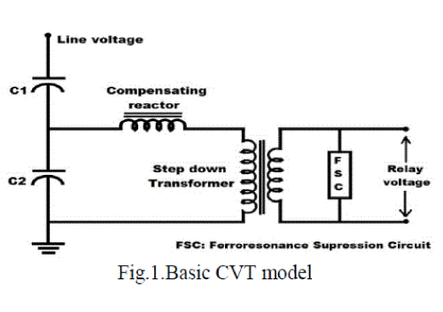
| The main components of CVT (as shown in Fig. 1.) are |
| i. stack capacitance which functions as a voltage divider to scale down the line voltage to an intermediate voltage |
| ii. tuning (compensating) reactor to compensate the reactance of the stack capacitance to avoid phase shift between the primary and secondary voltages at system operating frequency |
| iii. step-down transformer(SDT) to further reduce the intermediate voltage to lower level which is fed to the relays and other equipment and |
| iv. ferroresonance suppression circuit to mitigate the ferroresonance oscillations [4,5,6,7]. |
 |
 |
 |
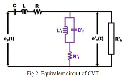
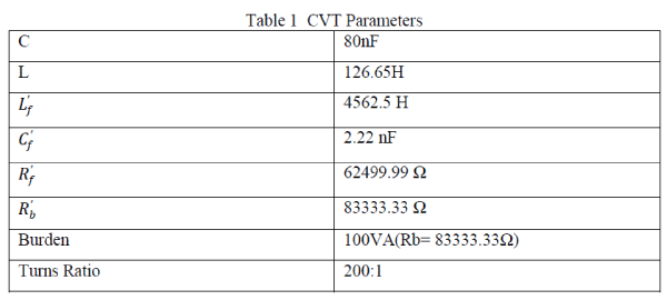
| The following are the parameters of the CVT considered in this paper. |
 |
CVT FREQUENCY RESPONSE
|
| The frequency response of CVT is represented by its gain (in decibels or dB) and phase angle ( in radians or degrees) plotted against frequency (in radians/sec or Hertz). These plots are known as the magnitude or amplitude response and the phase angle response respectively. In general, a magnitude gain of unity (1.0) and phase angle shift of zero (0°) degrees for the wide range of frequencies is an ideal frequency response. For CVT, it is difficult to obtain the ideal frequency response. |
| The gain curve is obtained by plotting the gain values at different frequencies according to the relationship: gain dB = 20*log10(gain), the unity gain (1.0) of ideal response is equivalent to zero gain in dB as 20*log10(1)= 0. The magnitude response of the CVT varies with the frequency, i.e. the gain is not constant at all frequencies. The gain curve is flat and represents the unity gain at normal operating frequency. Hence, the performance is good under the steady state condition. However, the response of CVT is deviating from unity gain for other frequencies. Therefore, the output signal is not an exact replica of the input signal for other frequencies. In this paper, to care of switching transients occuring in the system, the frequency response of CVT is considered up to 10kHz. |
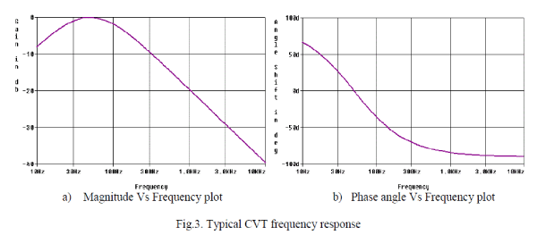 |
| The typical magnitude response of the CVT is shown in Fig. 3(a). At normal operating frequency, the gain curve is flat and unity i.e, the output signal is same as the scaled down input signal. For the sub synchronuos frequencies, the gain is less than unity i.e., the output signal is less than the input signal in terms of magnitude. There is attenuation in the output signal for DC and sub synchronous components of the signal. For the higher order frequencies the attenuation is more. |
| The phase response of the CVT is shown in Fig. 3(b). The phase response of the CVT varies with the frequency. For the rated frequency there is no phase difference between the input and output signal i.e., zero phase shift(0°). In case of sub synchronuos frequencies, the output signal leads the input signal in phase. In case of higher order frequencies, the output signal lags the input signal. The phase curve is almost linear till 300Hz and it remains almost constant for frequencies above 300 Hz. |
FACTORS INFLUENCING THE CVT FREQUENCY RESPONSE
|
| There are three major factors that influence the CVT frequency response [4,5]: |
| i. Ferroresonance Suppression Circuit (FSC) |
| ii. CVT Design parameters |
| iii. Burden. |
A) Ferroresonance Suppression Circuit
|
| The FSC is one of the major components which affects the frequency response of CVT. There are two types (active FSC and passive FSC) of FSC designs widely used [1, 6]. The active type of FSC comprises of inductance, capacitance and loading resistor. This forms an LC parallel circuit in series with resistor tuned to fundamental frequencies at which it offers very high impedance. The permanent connection of the active type FSC gives undesirable frequency response for other system harmonic frequencies. The passive FSC consists of saturable inductor (150% of normal voltage) and loading resistor which remains inactive, i.e. “passive”, for all conditions other than the ferroresonance. Therefore, the frequency response of passive FSC is better than active FSC. |
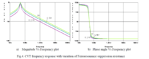
| The resistance value of the ferroresonance suppression circuit is another factor that influences the frequency response of CVT. Generally, the value of ferroresonance suppression resistance (Rf) is less than the burden. Hence, it will have loading effect on the CVT. The active FSC is considered for studying the effect of Rf on the CVT frequency response. The Fig. 4(a). shows the magnitude response of the CVT with different ferroresonance suppression resistances.The lower value of Rf results in more attenuation of the output signal and the magnitude curve improves with the increase in the Rf value, i.e., the loss of signal is reduced with higher value of Rf. |
| The output singnal leads the input signal for the sub synchronous frequencies and it lags the input signal for higher order frequencies as shown in Fig. 4(b). The phase response of CVT is comparitively better with increase in Rf value for non fundamental frequencies. It is observed that the magnitude and phase responses of the CVT improves with increase in the value of the ferroresonance suppression resistance. However, the change in the phase response is minimal with the change in Rf value. |
 |
B) CVT Design parameters
|
| The various design parameters of CVT that have influence on its frequency response are: |
| A. Ratio of Step Down Transformer |
| The increase in the turns ratio of the step down transformer will result in higher value of secondary current for a given burden impedance and increase in the loading of step down transformer[4]. Therefore, for a given burden, the increase in the turns ratio results in better magnitude response. |
| B. Stack capacitance |
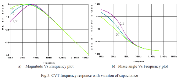
| The frequency response with the variation of the value of capacitance is shown in Fig. 5. For sub synchronous frequencies, the magnitude response is better with increase in the value of capacitance as shown in Fig. 5(a). The increase in the capacitance value gives better phase response for sub synchronous frequencies as shown in Fig. 5(b). It is observed that there is no change in the magnitude and phase response with the variation of capacitance for the higher order frequencies. |
 |
C) BURDEN
|
| The burden which is generally connected external to the CVT is also plays a significant role in determining its frequency response [1,6,8]. The effect of composition (power factor) and magnitude of the burden are considered for study. |
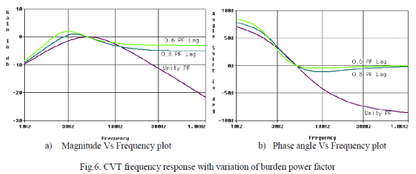 |
| The effect of the burden power factor on frequency response of the CVT is shown in Fig. 6. Generally, the unity power factor burdens or 0.8 lagging power factor burdens are used in the field. The 0.6 lagging power factor burden is considered for illustrative purpose only. The magnitude response is better in case of burden with lower power factor as shown in Fig.6.(a). The phase response improves with the increase in burden power factor for sub synchronous frequencies but the phase response worsens with increase in burden power factor for higher order frequencies as shown in Fig.6(b). |
| In case of 0.8 lagging power factor burden for certain range of sub synchronous frequencies, the gain curve crosses the zero dB point i.e. the gain is more than unity. The gain curve is becoming flat for frequencies more than 50Hz. In case of unity power factor burden, the gain curve is flat and unity for the normal operating frequency and the attenuation is more for higher frequencies compared to other power factor burdens. |
| In case of unity power factor burden there is comparitively lower phase shift for sub synchrnous frequencies but the phase shift is comparitively more for higher order frequencies. For 0.8 lagging pf burden, there is comparatively more phase shift observed for sub synchronous frequencies but the phase shift is comparitively lesser and remains almost constant for higher frequencies. |
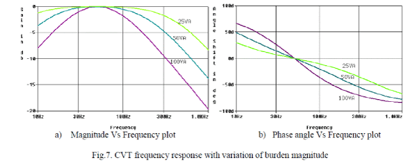 |
| The effect of burden magnitude (VA with unity power factor) on frequency response of the CVT is shown in Fig. 7. The Fig.7(a) infers that the magnitude response of the CVT is becoming flat for wide frequency band near the rated frequency by decrease in the burden VA. The Fig. 7(b) infers that the shift in the phase angle is decreasing and becoming flat near the rated frequency by decrease in the burden VA. The magnitude and phase responses of the CVT are improving with decrease in the VA of the burden as shown in Fig.7(a) and Fig. 7(b). |
CONCLUSION
|
| This paper demonstates the detailed response of the CVT in frequency domian and the effect of various factors influencing its frequency response. The factors which influence the CVT frequency response are type of ferroresonance suppression circuit and its damping resistance value, transformation ratio of SDT, value of stack capacitance and the composition and magnitude of burden. From the simulation study in this paper, we can conclude that the passive FSC with high value of ferroresonance suppression resistance, high SDT transformation ratio and stack capacitance, lower burden VA can aid in the better frequecny response of CVT. The 0.8 lagging power factor burden gives better frequency response for higher order frequencies than unity power factor burden. |
ACKNOWLEDGEMENTS
|
| The authors thank the management of Central Power Research Institute for permitting the publication of this paper. |
References
|
- DharmeshYelamanchi, JawaharAnnabattula and T.S.Sirish, “Analysis of Transient Performance of Capacitive Voltage Transformer”, Proceedings of National High Voltage Engineering Conference-2014,CPRI,Hyderabad, March,2014.
- “Transient Response of Coupling Capacitor Voltage Transformers IEEE Committee Report”, IEEE Transactions on Power Apparatus and Systems, Vol. PAS-100, No. 12, December 1981, pp. 4811-4814.
- Manual of Capacitor Voltage Transformer, Trench Limited, Instrument Transformer Division, Ontario, Canada, 2004.
- Sweetana, A., “Transient Response Characteristics of Capacitive Potential Devices”, IEEE Transactions on Power Apparatus and Systems, Vol. PAS-90,September/October 1971, pp. 1989-2001.
- Kezunovic. M., Fromen.C.W. and Nilsson. S.L., “Digital Models of Coupling Capacitor Voltage Transformers for Protective Relay Transient Studies”, IEEE Transactions on Power Delivery, Vol. 7, No. 4, Oct 1992, pp. 1927-1935.
- Kojovic. LJ.,Kezunovic. M. and Fromen. C.W., “A New Method for the CCVT Performance Analysis Using Field Measurements, Signal Processing and EMTP Modeling”, IEEE Transactions on Power Delivery, Vol. 9, No. 4, Oct 1994, pp.1907-1915.
- Lucas. J.R., McLaren. P.G., Keerthipala. W.W.L. and Jayasinghe. R.P., “Improved Simulation Models for Current and Voltage Transformers in Relay Studies”, IEEE Transactions on Power Delivery, Vol. 7, No. 1, January 1992, pp.152-159.
- Kasztenny. B., Sharples. D., Asaro. V. and Pozzuoli. M., “Distance Relays and Capacitive Voltage Transformers – Balancing Speed and Transient Overreach”, General Electric Company, GER-3986, 2000.
|