Digital Mobile Communication Systems are prevalent worldwide for providing data/voice services. Second generation systems are limited to the maximum data rate they can support. Third generation Mobile communication systems provide more advanced services such as broadband internet access, video telephony and video conferencing services. It integrates a wide variety of communication services such as high speed data, video and multimedia traffic as well as voice signals. In the Third Generation (3G) Cellular Systems, one of the most important and complex parts in the receiver is a carrier synchronization unit. The data is transmitted in a frame by frame basis through a time varying channel. The phase and frequency of the transmitted signal may also be shifted because of fading and the Doppler frequency shift. In receiver side, carrier frequency of the receiver should be synchronized with the incoming signal. In this paper, we designed, low complexity, adaptive baseband receiver carrier synchronization architecture for uplink wide band code order soma division multiple access (WCDMA) system based on 3rd Generation Partnership Project(3GPP) radio access network Frequency Division Duplex (FDD) mode specification and its Field Programmable Gate Array ( FPGA) Simulation is presented.
Keywords |
| 3G Cellular Systems, WCDMA Receiver, Scrambling codes, FPGAs. |
INTRODUCTION |
| The goal for the next generation mobile communications system is to seamlessly provide a wide variety of
communication services to anybody, anywhere, anytime. The intended service for next generation mobile phone users
includes services like transmitting high speed data, video and multimedia traffic as well as voice signals. The
technology needed to tackle the challenges to make these services available is popularly known as the Third/Fourth
Generation (3G/4G) Cellular Systems. |
| The first generation systems are represented by the analog mobile systems designed to carry the voice
application traffic. Their subsequent digital counterparts are known as second generation cellular systems. Third
generation systems make a significant leap, both in applications and capacity, from the current second generation
standards. Whereas the current digital mobile phone systems are optimized for voice communications, 3G
communicators are oriented towards multimedia message capability. |
| The first generation cellular systems generally employ analog Frequency Modulation (FM) techniques. The
Advanced Mobile Phone System (AMPS) is the most notable of the first generation systems. An AMP was developed
by the Bell Telephone System. It uses FM technology for voice transmission and digital signalling for control
information. |
| The second generation systems take the advantage of compression and coding techniques associated with digital
technology. All the second generation systems employ digital modulation schemes. Multiple access techniques like
Time Division Multiple Access (TDMA) and Code Division Multiple Access (CDMA) are used along with FDMA in
the second generation systems. The Third/Fourth generation cellular systems are being designed to support wideband
services like high speed Internet access, video and high quality image transmission with the same quality as the fixed
networks. |
| In this paper, an uplink base band receiver architecture conforming to the 3GPP RAN FDD-mode WCDMA
standard is proposed. This architecture includes a beam former using correlator based beam searcher, a four finger rake
combiner, a matched filter based channel estimator and a carrier synchronization loop. Simulations based on two
Doppler fading multipath channel models specified in the 3GPP standard document. The proposed beam forming
receiver architecture can accommodate up to 15 users with 60-kbps channel bit rate at a frequency offset of 200Hz ,an
SNR of 0db,a speed of 120 km/h and the desired user’s power as low as -10dB relative to that of interfering users. An
FPGA emulation of the proposed architecture to operate at a sample rate of 15.36MHz, as fast as that specified by the
standard. The proposed architecture serves as a solid foundation for future cost effective application-specific integrated
circuit (ASIC) implementation of the baseband processing circuit in a WCDMA base station receiver. We developed
the simulator for a WCDMA system operating in the FDD mode. |
SYSTEM MODEL AND ASSUMPTIONS |
| In this scheme, the radio access network of a WCDMA system operating in the (Frequency Division Duplex(FDD)
mode is described and the spreading & modulation operation for the Dedicated Physical Channels (DPCH) at both the
links is illustrated in detail since it is the most essential part of the simulator that we implement. The uplink and
downlink data structure along with spreading and scrambling codes used in both the links for the DPCHs is described.
The spreading modulation and data structure for Physical Random Access channel (PRACH), Synchronization Channel
(SCH) etc. are described in detail in and along with those of the DPDCHs. |
| In the uplink the data modulation of both the DPDCH and the DPCCH is Binary Phase Shift Keying (BPSK).
The modulated DPCCH is mapped to the Q-channel, while the first DPDCH is mapped to the I-channel. Subsequently
added DPDCHs are mapped alternatively to the I or the Q channel. Spreading Modulation is applied after data
modulation and before pulse shaping. The spreading modulation used in the uplink is dual channel QPSK. Spreading
modulation consists of two different operations. The first one is spreading where each data symbol is spread to a
number of chips given by the spreading factor. This increases the bandwidth of the signal. The second operation is
scrambling where a complex valued scrambling code is applied to spread signal. The bipolar data symbols on I and Q
branches are independently multiplied by different channelization codes. The channelization codes are known as
Orthogonal Variable Spreading Factor (OVSF) codes. |
| Quaternary Phase Shift Keying (QPSK) is applied for data modulation in the downlink. Each pair of two bits is
serial-to-parallel converted and mapped to the I and Q branches respectively. The data in the I and Q branches are
spread to the chip rate by the same channelization code. This spread signal is then scrambled by a cell specific
scrambling code. The downlink user has a DPDCH and a DPCCH. Additional DPDCHs are QPSK modulated and
spread with different channelization codes. We can observe some differences between the spreading and modulation in
the downlink and that in the uplink. The data modulation is QPSK in downlink whereas it is BPSK for the uplink. The
data rates in the I and Q-channels are the same in the downlink whereas data rates in the I and Q-channel of the uplink
may be different. The scrambling code is cell specific in the downlink, whereas it is mobile station specific in the
uplink. |
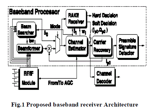
PROPOSED BASEBAND RECEIVER ARCHITECTURE |
| In this scheme, a four-element antenna array is adopted in the proposed uplink receiver. The baseband receiver takes
eight input signals (I and Q channels per antenna element) from the RF/IF module and generates hard decisions or soft
decisions for the optional channel decoder. Single baseband receiver architecture can be used for signal detection of all
three uplink physical channels mentioned above, due to the similarity in the transmission scheme of the Physical
Random Access Channel (PRACH) message part (data and control port) and the Dedicated Physical Channel (DPCH).
Furthermore, DPCH is divided into one data channel and one control Channel. Dedicated Physical Data Channel
(DPDCH) and Dedicated Physical Control Channel (DPCCH). |
 |
| I. CARRIER SYNCHRONIZATION LOOP |
| Due to fading and local oscillator frequency mismatch, the phase of the incoming signal must be compensated
appropriately for both DS & FH spread system a receiver must be employed a synchronized replica of the spreading
signal to demodulate the received signal successfully. The process of synchronizing the locally generated spreading
signal with the received signal us usually accomplish in carrier synchronization unit. |
| It has two steps to implement the carrier synchronization. |
| 1. ACQUISITION: Bring the two spreading signal in to rough alignment with one another. |
| 2. TRACKING: Takes over and continuously maintains the best possible waveform fine alignment by means of a
feedback loop. |
| The acquisition problem is one of searching throughout a region of time and frequency uncertainty in order to
synchronize the received spreading signal with the local generator spreading signal. When determining the limits of
uncertainty in time and frequency the following points to be considered. |
| • Uncertainty in distance between the Transmitter and Receiver translates into uncertainty in the amount of propagation
delay. |
| • Relative clock instability between transmitter and receiver results in Phase difference between the Transmitter (Tx)
and Receiver (Rx) spreading signals. That will tend to grow as a function of elapsed time between synchronization. |
| • Uncertainty of the Rx relative velocity with respect to the Transmitter, Translates into uncertainty in the value of the
Doppler frequency shift of the incoming signal. |
| • Relative oscillator in stability between Transmitter and Receiver result in frequency offset (shift) between the two
signals. |
| ACQUISITION UNIT- A common feature of all acquisition methods is that the received signal and the locally
generated signal are first correlated to produce a measure of similarity between the two. This measure is then compared
with a threshold to decide if the two signals are in synchronization if there are the tracking loop takes over. If there are
not the acquisition procedure provide for a phase or frequency change in a locally generator PN code as a parameter of
systematic search through the receiver phase and frequency uncertainty region and another correlation is attempted. |
| TRACKING UNIT- The loop provides the fine synchronization by first generated 2 PN sequence g(t) g(t+τ) delayed
from each other by one chip. |
CARRIER SYNCHRONIZATION CIRCUIT FOR PROPOSED ARCHITECTURE |
| A carrier synchronization phase-locked loop is adopted in the proposed receiver. The loop operates in two modes:
acquisition mode and tracking mode. In the acquisition mode, which happens during the reception of the PRACH
preamble, an average of the phase difference between two consecutive symbols is calculated and used as an estimation
of the frequency offset. In the tracking mode, enabled during a DPCCH/DPDCH reception, the whole carrier
synchronization loop begins to operate. A common feature of all acquisition methods is that the received signal and the
locally generated signal are first correlated to produce a measure of similarity between the two. This measure is then
compared with a threshold to decide if the two signals are in synchronization if there are the tracking loop takes over. |
| Once Acquisition is completed tracking is taking place. Tracking maintains the line synchronization .The
locally generated code of the tracking loop is offset in the phase from the incoming signal S (t) by the time phase where
Æ is less than Tc/2.In the tracking mode, enabled during a DPCCH/DPDCH reception, the whole carrier
synchronization loop begins to operate. |
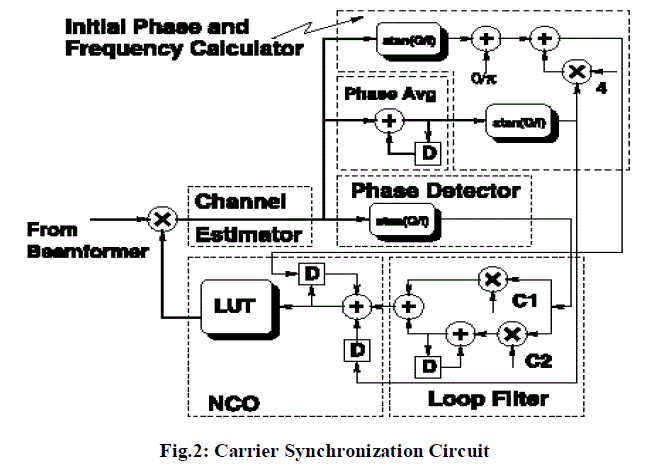 |
| The phase detector calculates the phase of the most significant peak in the matched filter output (Ip0 ,Qp0 )
supplied from the channel estimator. The loop filter is a conventional proportional-and-integrate type and a
numerical-controlled oscillator (NCO) is adopted in this digital phase-lo clocked loop. |
| In the carrier synchronization circuit, the initial phase/frequency calculator operates only once during the
PRACH preamble, while the phase detector and the loop filter operate at symbol rate and the NCO. |
RESULT AND DISCUSSION |
| With the advent of VLSI technology, designers could design single chips with more than 100,000 transistors. Because
of complexity of these circuits, it was not possible to verify these circuits on a breadboard. Computer aided techniques
became critical for verification and design of VSLI digital circuits. Computer programs to do automatic placement and
routing of circuit layouts also became popular. Logic simulators came into existence to verify the functionality of these
circuits before they were fabricated on the chip. |
| VHDL is an offshoot of the very high-speed integrated circuit (VHSIC) program to describe hardware from the
abstract to the concrete level. VHDL is rapidly being embraced as the universal communication medium of design. In
the direct sequence serial search acquisition & Tracking, the following algorithm is used. |
| Algorithm: Acquisition |
| 1. First generate the PN sequence. |
| 2. Multiply and accumulate the locally the generated sequence with received PN sequence |
| 3. If the accumulated result is not equal to the number of sequences used in the PN sequence. |
| 4. Again generate the PN sequence with one clock pulse delay and multiply and accumulate with the received PN
Sequence. |
| 5. If the accumulated result is not equal to the number of sequences used in the PN sequence. |
| 6. The repeat the step 4 until the accumulated result is equal to the number of sequence used the PN sequence. |
| Algorithm: Tracking |
| 1. First generate the two PN sequence with Tc phase change. That is g(t+τ+Tc/2) and g(t+τ-Tc/2). |
| 2. Compare the Phase different with incoming PN sequence (received). |
| 3. If the phase difference is constant .The PN sequence with g (t+τ) is generated for data reception. |
| 4. If there is Phase different, then verify if the phase difference is lead or lag. |
| 5. If it is lead, then reduce the value of t accordingly phase of the locally generated PN sequence is synchronized with
the Incoming sequence. |
| 6. If it is lagging, then increase the value of t accordingly phase of the locally generated PN sequence is synchronized
with the Incoming sequence. |
| Simulation Results |
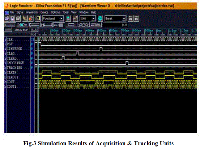 |
| Fig.3 shows that detection of accumulated result is not equal to the number of sequences used in the PN sequence and
synchronization with Incoming sequence or data received. |
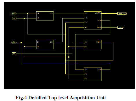 |
| Fig.4 and Fig.4 gives the detailed digital architectures for the proposed design. |
CONCLUSION |
| Thus, it Proposed an uplink base band receiver architecture conforming to the 3GPP RAN FDD-mode WCDMA
standard and this architecture includes a beam former using correlator based beam searcher, a four finger rake
combiner, a matched filter based channel estimator and a carrier synchronization loop. Simulations were conducted
based on two Doppler fading multipath channel models specified in the 3GPP standard document. Moreover, in order
to test the advanced features provided by proposed beam former, vector channel models derived from the scalar
channels described in the standard were also used. The simulation results showed that the proposed beam forming
receiver architecture can accommodate up to 15 users with 60-kbps channel bit rate at a frequency offset of 200Hz ,an
SNR of 0db,a speed of 120 km/h and the desired user’s power as low as -10dB relative to that of interfering users. |
| FPGA emulation of the proposed architecture was also conducted. The emulation can be operated at a
sample rate of 15.36MHz, as fast as that specified by the standard. Moreover the measured results show identical
performance to those obtained in the circuit simulation, verifying the feasibility of the proposed architecture. Therefore
the proposed architecture serves as a solid foundation for future cost effective Application-Specific Integrated Circuit
(ASIC) implementation of the baseband processing circuit in a WCDMA base station receiver. |
References |
- R. TANNER AND J. WOODARD, EDS., WCDMA REQUIREMENTS AND PRACTICAL DESIGN, JOHN WILEY & SONS,2009.
- B.J. Minnis and P.A. Moore, .A Highly Digitized Multimode Receiver Architecture for 3G Mobiles,.IEEE Transactions on Vehicular Technology, vol. 52, no. 3, pp. 637.653, May 2008.
- R. H. M. van Veldhoven, .A Triple- Mode Continuous-Time ̢̤̉̉ Modulator With Switched-Capacitor Feedback DAC for a GSMEDGE/ CDMA2000/UMTS Receiver,.IEEE Journal of Solid-State Circuits, vol. 38, no. 12, pp. 2069. 2076, December 2008
- 3GPP TSG RAN WG1, Physical Channels and Mapping of Transport Channels on to Physical Channels (FDD), TS 25.211 v3.4.0 Oct.2009.
- D.Koulakiotis and A.II.Aghvami,âÃâ¬ÃÂData detection techniques for DS/CDMA mobile system: A review,âÃâ¬ÃÂIEEE Personal Communication, vol.7no.3, pp24-34, June 2008
- A. Morrison and B.S.Sharif,âÃâ¬ÃÂA space-time beam forming RAKE receiver for 3G WCDMA base station,âÃâ¬ÃÂIEEE International Conference on consumer Electornics, pp 312-313, 2008.
- E.S Shin and Y.O.Park,âÃâ¬ÃÂDesign and anaysis of a smart antenna system for IMT 2000 W-CDMA,âÃâ¬ÃÂVTC 99, vol 49,no.3, pp.2109-2112, 2007.
- 3GPP TSG RAN, Base Station conformance testing (FDD), TS 25.141 V3.3.0 Oct 2007
- M.Suzuki, M.Kawabe and N.Doi, âÃâ¬ÃÅA Proposal of new architecture for W-CDMA baseband LSIâÃâ¬ÃÂ, VTC 99, vol 49.
- L.Philips,N.Lugil, and J.Vanhoof , âÃâ¬ÃÅA baseband IC for 3G UMTSCommunicationsâÃâ¬ÃÂ,VTC 99,vol 50,no.3, pp 1521-1524,2007.
- http://www.ijettjournal.org/volume-4/issue-6/IJETT-V416P180.pdf
|