Once the I2C protocol designed for data surveillance system, It is easy to communicate devices with each other without data loss, as well as a excellent speed is being developed with I2C as compare to any other communication methodology. Security is a vital issue that expands across many areas of life that require protecting vital information, goods, or areas from those who would want to trespass or steal. The Primary objective of our project is to design a basic security system that would be able to track objects moving across the view of the camera. This design method was design in VHDL, implementation in FPGA and applied in OV7620 single-chip CMOS VGA color digital camera
Keywords |
| I2C protocol, Data surveillance, FPGA, VHDL SDA, SCL, OV7620 |
INTRODUCTION |
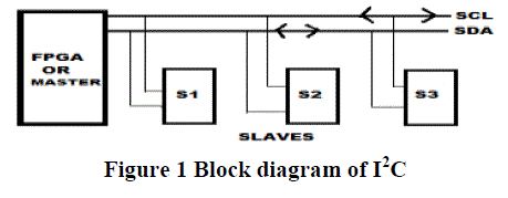
| The I2C bus is two wires, low to medium speed communication bus which reduces the manufacturing cost of electronics
products. It provide low cost but powerful chip to chip performance will be affected under complex electromagnetic
environment by the improper for Audio/Video surveillance first presented and then technical description of I2C protocol
implementation is followed. Continuous monitoring of the area under surveillance is done by taking the video of the place.
The video is captured using a CMOS sensor in the form of frames. These frames are stored and compared and the variation
between any two frames is calculated. When there is no intrusion, the variation is zero. When any movement detect then the
size of the moving object will calculate if the size of the object is more than the specific value at this situation the level of
threat will be so high. This would enable a security system that wouldn't require manpower until it detected an intrusion. |
 |
DIFFERENT STAGES TO INTERFACING THE DEVICES |
| With the I2C protocol interfacing the device having four basic stages, with these four conditions devices has to configure to
the MASTER or FPGA board. |
| • I2C Bus Events: The START and STOP conditions |
| • I2C Bus Events: Transmitting a byte to a receiver |
| • I2C Bus Events: Getting Acknowledge from a receive |
| • I2C Bus Events: Receiving a byte from a Receive |
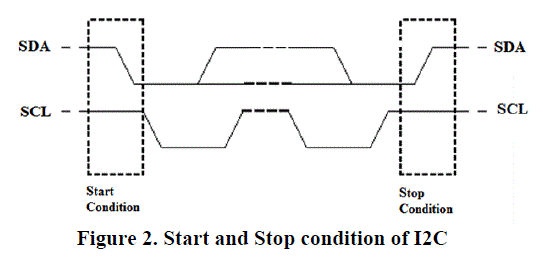 |
| 2.1. I2C Bus Events: The START and STOP Conditions -Prior to any transaction on the bus, a START condition needs
to be issued on the bus. The start condition acts as a signal to all connected IC's that something is about to be transmitted on
the bus. As a result, all connected chips will pay attention to the bus. After a message has been completed, a STOP
condition is sent. This is the signal for all devices on the bus that the bus is available again (idle). If a chip was accessed
and has received data during the last transaction, it will now process this information (if not already processed during the
reception of the message). |
| START-The chip issuing the Start condition first pulls the SDA (data) line low, and next pulls the SCL (clock) line low.
STOP-The Bus Master first releases the SCL and then the SDA line.
A single message can contain multiple Start conditions. The use of this so-called “repeated start" is common in I2C.A Stop
condition ALWAYS denotes the END of a transmission. Even if it is issued in middle of a transaction or in the middle of a
byte. It is "good behavior" for a chip that, in this case, it disregards the information sent and resumes the "listening state",
waiting for a new start condition. |
| 2.2 I2C Bus Events: Transmitting a byte to a receiver-Once the start condition has been sent, a byte can be transmitted
by the MASTER to the RECEIVER First byte after a start condition will identify the receiver on the bus (address) and will
select the mode of operation. The meaning of all following bytes depends on the receiver. A number of addresses have been
reserved for special purposes. One of these addresses is reserved for the "Extended Addressing Mode". As the I2C bus
gained popularity, it was soon discovered that the number of available addresses was too small. Therefore, one of the
reserved addresses has been allocated to a new task to switch to 10-bit address is mode. If a standard receiver (not able to
resolve extended addressing) receives this address, it won't do anything (since it's not its address).If there are receivers on
the bus that can operate in the extended 10-bit addressing mode, they will ALL respond to the ACK cycle issued by the
master. The second byte that gets transmitted by the master will then be taken in and evaluated against their address. Even
in 10-bit extended addressing mode, Bit 0 of the first byte after the Start condition determines the receiver access mode ('1'
= read / '0' = write). |
| 2.3 I2C Bus Events: Getting Acknowledge from a receive - When an address or data byte has been transmitted onto the
bus then this must be ACKNOWLEDGED by the receiver(s). In case of an address: If the address matches its own then that
receiver and only that receiver will respond to the address with an ACK. In case of a byte, transmitted to an already
addressed receiver then that receiver will respond with an ACK as well. The receiver that is going to give an ACK pulls the
SDA line low immediately after reception of the 8th bit transmitted, or, in case of an address byte, immediately after
evaluation of its address. In practical applications this will not be noticeable. This means that as soon as the master pulls
SCL low to complete the transmission of the bit. |
| • SDA will be pulled low by the receiver |
| • master now issues a clock pulse on the SCL line |
| • The receiver will release the SDA line upon completion of this clock pulse |
| • The bus is now available again for the master to continue sending data or to generate a stop condition. |
| In case of data being written to a receiver, this cycle must be completed before a stop condition can be generated. The
receiver will be blocking the bus (SDA kept low by receiver) until the master has generated a clock pulse on the SCL line |
| 2.4 I2C Bus Events: Receiving a byte from a receiver -Once the receiver has been addressed and the receiver has
acknowledged this, a byte can be received from the receiver if the R/W bit in the address was set to REID (set to '1'). The
protocol syntax is the same as in transmitting a byte to a receiver, except that now the master is not allowed to touch the
SDA line. Prior to sending the 8 clock pulses needed to clock in a byte on the SCL line, the master releases the SDA line.
The receivers will now take control of this line. The line will then go high if it wants to transmit a '1' or, if the receiver
wants to send a '0', remain low. |
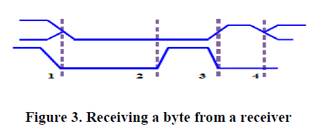 |
| All the master has to do is generate a rising edge on the SCL line (2), read the level on SDA (3) and generate a falling edge
on the SCL line (4). The receiver will not change the data during the time that SCL is high. (Otherwise a Start or Stop
might inadvertently be generated.) During (1) and (5), the receiver may change the state of the SDA line. In total, this
sequence has to be performed 8 times to complete the data byte. Bytes are always transmitted MSB first. The meaning of
all bytes being read depends on the receiver. There is no such thing as a “universal status register". You need to consult the
data sheet of the receiver being addressed to know the meaning of each bit in any byte transmitted. |
THEORY RELATED TO WORK |
| The I2C protocol is level-sensitive. The data must be stable when SCL is high. Except for two situations, the state of the
SDA line can only change when SCL is low. The exceptions have special meaning. 1-to-0 transition signals the beginning
of a transfer and is termed as a start condition. A 0-to-1 transition signals the end of a transfer and is termed as a stop
condition. The data is transferred in bytes, with the most significant bit sent first. The byte transfer requires nine clock
pulses. The transfer of a byte‟s bits takes eight pulses, and the ninth is used for acknowledgment. Between start and stop
conditions, an unrestricted number of bytes can be transferred. The communication in between the devices is very simple
but before interfacing Master as well as Slave checks some condition of follows the condition only the device is being
interface. The interfacing need several condition like SATRT1,ACK2,Device Id3,Register location address4, Register data5
and finally the STOP6. After a start condition, the byte containing the slave address (or part of the address, when 8-bit
addressing is used) and a data direction bit is always sent first. A start condition can be repeated without first generating a
stop condition. This is used to change transfer direction or to address another slave. If there is no acknowledgment from the
addressed slave (because it is not connected or performs some internal operation), the master can abort the transfer. Next, i f
the slave is being written to, it must acknowledge each byte received. Lack of acknowledgment indicates that it cannot
accept data. While reading from the slave, the master is also obliged to acknowledge each byte, except the last byte. The
master can communicate with the slave according to several scenarios called transfer formats. |
 |
| START from the SDA line, the position of the SDA line first High to Low means 1 to 0 and after some Pico second the
position of the SCL line is High to Low means 1 to 0. It means a FPGA send the start signal to slaves that Master (FPGA)
is ready for further communication. |
| ACK- After every byte to be transmitted by Mater or Slave a ACK signal can be transmitted by other device ,ACK signal
means whatever the device is being transmitted can be properly received by other device properly. |
| Device Id- The device Id is fixed for every device hat can e interface on the FPGA.The Id for more than one system cannot
be match. The Id is 8 bit long and it can be transmitted in series means one by one..The Id is 8 bit long means total 256
devices are to be interface. For adding more than 256 devices the bit is being increased. |
| Register Address-Register address is 8 bit long, it indicate that total 256 locations for a register is available to be
controlled. Each individual register is properly interface by I2C protocol. |
| Register Data- Register data is also 8 bit long,the is help us to controlled the value of the parameter to be controlled. |
| Stop-After Id, Register Address, Register data a stop signal is being transmitted by FPGA. It indicate that a cycle of one
transition is completed |
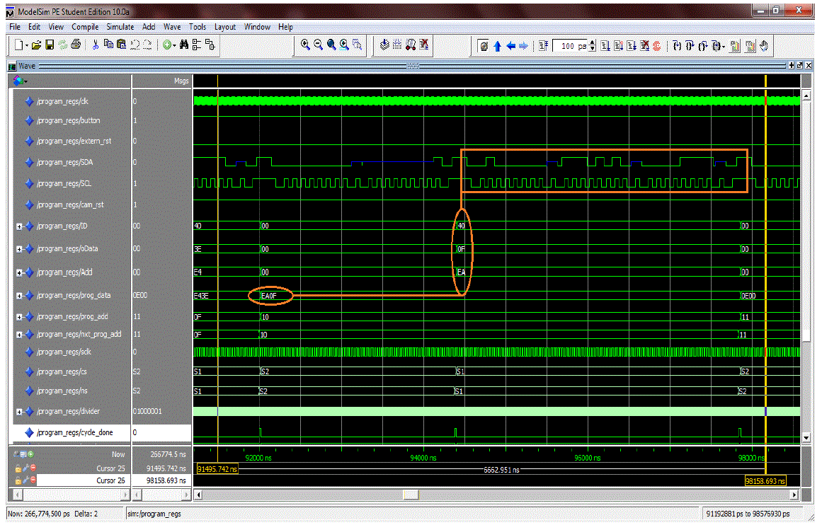
| 3.1 Ist Stage Transition – The transition is start from clk line, the clock is around 100 ps will be provided to the system,
The position of the butten is set to 1 by forcing the value and the position of the external_rst will be 1,the transition being
started but it is blank transition. The proper transition started only when the value of external_rst is forced by 0 while
forcing the value suddenly the the SDA line goes High to Low means 1 to 0 after a few instant SCL line also goes High to
Low means 1 to 0.indicate that FPGA start sending the START signal to all interfaces Slaves . When this start signal get
collected by Slaves, the start sending the ACK signal.This ACK signal will be received by the FPGA, the actual
transmission will be start .The communication is serial communication technique and value can be change for every rising
edge of the SCL line. |
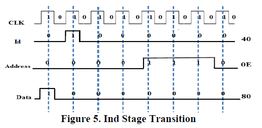
| The ACK received by FPGA,a Slave start sending device Id i.e. 40H[0100 0000] every bit of the device Id interchange
serially one by one and the states will be change for every rising edge like [Low-High-Low-Low-Low-Low-Low-Low].
After the device Id being send by Slaves and received by FPGA receiver sends the ACK signal after receiving the ACK
signal the Address of the register is ready for sending i.e 3A [0011 1010] every bit of the device Id interchange serially one
by one and the states will be change for every rising edge like [Low- Low- High- High- High- Low- High-Low].When the
Register is properly build up to the FPGA, receiver again send the ACK signal after this Slave start sending data i.e
16[0001 0110] every bit of the device Id interchange serially one by one and the states will be change for every rising edge
like [Low- Low-Low- High-Low- High- High-Low].The data of the Register decide decide the parameter which want to
controlled but the device Id and the Address of the Register is fixed. |
| The formula is: |
| PS_gain=1+ (PS<7:0> - [80])/[100]; range (0.5x ~ 1.5x). |
| PS<7> - Sign bit. If “1”, PS channel gain increase; “0” gain decrease. |
 |
RTL DESCRIPTION |
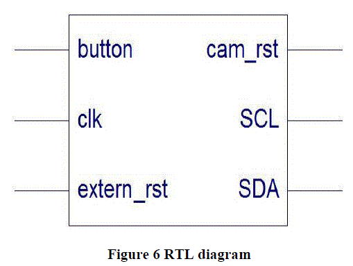
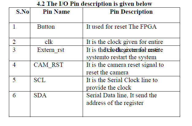
| -A RTL diagram of I2C is shown in figure..A result can be verified on ModelSim and effective and high speed
communication link can be implemented and verified. The input values can be forced and Output
3A16(0011,1010,0001,0110),5004(0101,0000,0000,0100),0E80(0000,1110,1000,0000) and the Id of the device is fixed i.e.
40(0100,0000)Hex. |
 |
 |
 |
| 4.4 - Advantage of Communication with I2C -FPGAs are particularly well suited to meet the requirements of many data
processing applications. FPGAs have the following characteristics that make them very appealing |
| High performance: HD processing can be implemented in a single FPGA. |
| Flexibility: FPGAs provide the ability to upgrade architectures quickly to meet evolving requirements, while scalability
allows use of FPGAs in low-cost and high-performance systems. |
| Low development cost: Data development kits from start as low as US$1,095 and include the software tools required to
develop a data system using FPGAs. Obsolescence proof: FPGAs have a very large customer base on ship products for
many years on. In addition, FPGA designs are easily migrated from one process node to the next. |
| Plan for lower production costs: offers several ways to help plan for the time when products move from lower unit
volumes to much higher volume |
CONCLUSION |
| The ideal surveillance architecture with I2C will have the following characteristics: high performance, flexibility, easy
upgradability, low development cost, and a migration path to lower cost as the application matures and volume ramps. 's
FPGAs in conjunction with the feature-rich Data and Image Processing Suite, Data over IP reference design, and partner's
compression solutions offer data system designers all the key building blocks needed to produce such a system. |
References |
- THE I2C BUS SPECIFICATION VERSION 2.1 January, 2000, Philips Semiconductors.
- Fred Eady “Networking and Internetworking with Microcontrollers” Elsevier, 2004.
- J. Bhasker, A VHDL Synthesis Primer, BS Publications 2nd Edition, 2003, pp. 132.
- TMS470R1x Inter-Integrated Circuit (I2C) Reference Guide, Texas Instruments (SPNU223).
- Design Ware Inter-IC (I2C) VIP Data book, Version 1.10a, February 18, 2005, Synopsis.Figure 6. Flow Summary of the Device 1.
- P.Venkateswaran, A. Saynal, S. Das, S.K Saynal and R. Nandi , “FPGA Based Efficient Interface Model for Scale-Free Computer Networking using I2C Protocol” 15th.intl‟conf on computing – CIC 2006, Proc. Research in Computing Science: Special Issues – Advances in Computer Science &Eng., ISSN 1870 – 406, pub .National Polytechnic Institute, Mexico, Vol.23, pp 191 -198 , Nov. 21-24,2006
- Xavier Righetti Xavier Righetti “Proposition of a Modular I2C-Based Wearable Architecture”IEEE-2010
- Jan O. Borchers, Wolfgang Samminger, Max M¨uhlh¨auser “Personal Orchestra: Conducting Audio/Video Music Recordings” IEEE-2002.
- A.R.M. Khan, A.P.Thakare, S.M.Gulhane “FPGA-Based Design of Controller for Sound Fetching from Codec Using Altera DE2 Board” International Journal of Scientific & Engineering Research,
- A.K. Oudjida, M.L. Berrandjia, R. Tiar, A. Liacha, K. Tahraoui „FPGA Implementation of I2C & SPI Protocols”a Comparative Study‟IEEE 2009
- J.M. Irazabel& S. Blozis, Philips Semiconductors, “I2CManual, Application Note, ref. AN10216-0” March 24, 2003.
- F. Leens, “An Introduction to I2C and SPI Protocols,” IEEE Instrumentation & Measurement Magazine, pp. 8-13, February 2009.
- L. Bacciarelli et al, “Design, Testing and Prototyping of a Software Programmable I2C/SPI IP on AMBA Bus,” Conference on Ph.D.Res
|