This paper proposes a Space Vector PWM (SVPWM) algorithm based on fractals for two legged three phase multilevel inverters. The paper presents the observation that the space vector representation of two legged three phase multilevel inverter has an inherent fractal structure. The properties of fractal structure together with the simplicity of fractal arithmetic are utilized to propose a generalized algorithm for SVPWM generation for two legged multilevel inverters and it can be easily extended to n-level inverters. The voltage space vectors of higher level inverter can be generated from the voltage vectors of an equivalent 2-level inverter using simple addition operations. Sector identification and switching vector determination in SVPWM generation are carried out using simple arithmetic operations without any computational complexity. The proposed algorithm doesn’t use any look up table for sector identification and switching vector determination. The validation of the algorithm through simulations in MATLAB/SIMULINK has been carried out for two legged 3-level and 5-level inverter configurations for which the results are also presented.
Keywords |
| Six-switch three phase inverter [SSTPI] topology, Four-switch three phase inverter [FSTPI] topology, Two
legged multilevel inverters, Space vector pulse width modulation [SVPWM], Fractals |
INTRODUCTION |
| Multilevel inverter technology has emerged as a powerful technique in the area of medium voltage high power
applications. Multilevel inverter synthesizes desired output voltage from multiple levels of dc voltages. As the number
of voltage level increases the harmonic content of output voltage waveform decreases significantly [1], [2]. Multilevel
inverters gained more attention in recent years due to its inherent advantages of high voltage handling and good
harmonic rejection capabilities with currently available power devices. The requirement of more number of
semiconductor switches is the major disadvantage of multilevel inverters. Although low voltage rated switches can be
used in a multilevel inverter, each switch requires a related gate drive protection circuits and the overall system
becomes more complex and expensive. In addition increased number of switches increases the switching losses and
electromagnetic interference (EMI). The increased switches have limited the usage of multilevel inverters in many
critical applications particularly in the field of aerospace applications. The reduction in the number of power
semiconductor switches for the inverters is drawing significant research attention. The four switch three phase inverter
topology [FSTPI] is one of the techniques to reduce the switches in the inverter [3]. Compared to conventional three
phase inverter with six switches [SSTPI], FSTPI has two switches in each two legs and one leg is replaced with
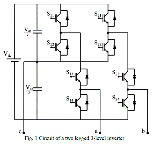
capacitors. The two legged 2-level inverter configuration is the four switch topology referred to in literature. Fig.1
shows the two legged 3-level inverter circuit. Space Vector Pulse Width Modulation (SVPWM) is the most popular and
best choice for generating PWM for multilevel inverters due to its inherent advantages of better fundamental output
voltage, reduced switching losses, lower harmonic distortion and easier implementation [4]-[11]. There has been
significant work in the area of Space vector PWM for four switch inverters [12]-[17] but the extension to multilevel
inverter configuration is yet to be explored. |
| The paper explores the possibility of extending the concept of SVPWM for FSTPI to multilevel configurations. The
paper begins with the space vector representation of two legged multilevel inverters and brings out the observation that
the voltage space vector representation of a two legged multilevel inverter has an inherent fractal structure with the
basic unit of this structure being the triangle made of the vertices of three adjacent inverter voltage space vectors [10].
The inherent fractal structure is utilized in the paper to propose a simple and generalized algorithm to generate
SVPWM for any two legged multilevel inverters. The paper presents the simulation results of the algorithm
implemented in MATLAB/SIMULINK for 3-level and 5-level inverter configurations. |
 |
INHERENT FRACTAL STRUCTURE IN THE SPACE VECTOR REPRESENTATION OF TWO LEGGED
MULTILEVEL INVERTERS |
| SVPWM utilizes the space vector concept for computing the duty cycle of the switches. Generation of SVPWM
involves approximating the instantaneous reference voltage space vector by switching the three nearest inverter voltage
vectors [9]. Fig. 2(a) shows the space vector representation of two legged 2-level three phase inverter and it may be
noted that the voltage space vector representation of two legged 2-level inverter has four inverter voltage vectors
located at the vertices of the parallelogram which be divided into two equilateral triangles (sectors) numbered as S1 and
S2. |
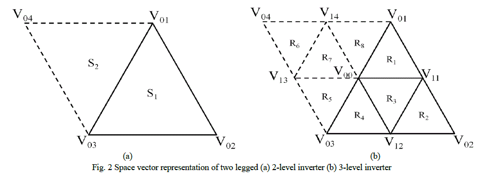 |
| Space vector representation of two legged 3-level inverter is shown in Fig. 2(b), where V01, V02, V03 and V04 are the
same as the locations of the voltage space vectors of 2-level inverter. It may be noted that 3-level inverter has five
additional voltage vectors and are located at V00, V11, V12, V13 andV14. Consider the region marked as S1 in the case of
2-level inverter [Fig. 2(a)], formed by the voltage vectors located at V01, V02 and V03. In the case of 3-level inverter
[Fig. 2(b)], this region has three additional voltage space vectors located at V00, V11 and V12 and is located at the
midpoints of each side of the triangle [ΔV01V02V03] of equivalent 2-level inverter. Hence the ΔV01V02V03 of 3-level
inverter consists of four sectors, formed by the voltage space vectors located at V01, V11, V02, V12, V03, V00. Also the
ΔV01V03V04 contains another four sectors. So the total number of sectors in 3-level two legged inverter is 8 [R1-R8] as
shown in Fig. 2(b). |
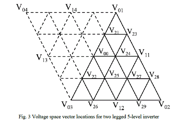 |
| Fig. 3 shows the voltage space vector locations for two legged 5-level inverter. In Fig. 3, in the case of the triangular
region formed by the voltage space vectors located at V01, V02 and V03, besides the voltage space vectors of 3-level
inverter, nine additional voltage space vectors are present and are located at V21, V22, V23, V24, V25, V26, V27, V28 and
V29. The nine additional voltage vectors are located at the midpoints of the sides of sectors of 3-level inverter and these
nine voltage vectors together with the voltage vectors of 3-level inverter results 16 sectors within ΔV01V02V03. By
considering the sectors in the ΔV01V03V04, total sectors formed for 5-level inverter becomes 32. In this manner, each
sectors formed by the voltage space vectors of 2-level inverter divided into four smaller sectors results the voltage
space vector representation of 3-level inverter with 8 sectors. All these 8 sectors of the 3-level inverter further divided
in to four smaller sectors and this results the voltage space vector representation of 5-level inverter with 32 sectors. The
process gets repeated as the number of level increases and the voltage space vector locations of any level can be
generated. Generalizing, the number of triangles for the two legged n level inverter can be obtained as, |
 |
| Whereas the number of triangles for the conventional n level inverter is, 6 × (n − 1)2 . Thus the number of triangles
for the two legged inverter configuration is only one-third of the number for conventional inverters. The advantage of
lesser triangles further simplifies the generation of SVPWM for two legged higher level inverters. |
| The space vector representation of 2-level inverter can be grows to that of higher level inverters by repeated division
of each sectors. At every stage due to the presence of additional voltage space vectors, each triangular sector is divided
into four smaller triangular sectors. On moving from 2-level vectors to 3-level each triangle in the space vector location
gets subdivided into four smaller triangles, which further subdivides for the 5-level inverter. The division of each
triangle into four smaller triangles by joining the midpoints of the sides of the triangle is the basis for Sierpinski
triangle generation in fractal theory. According to fractal theory, it may be noted that the switching voltage space vector
representation of two legged multilevel inverter has a fractal structure with the basic structure is a triangle. In the present work this observation is used to propose a generalized algorithm for the SVPWM generation for any two legged
n-level configuration. The switching voltage vectors and switching states of higher level inverters can be generated
from an equivalent 2-level inverter using repeated triangularization algorithm [10]. |
GENERALIZED SVPWM ALGORITHM FOR TWO LEGGED MULTILEVEL INVERTERS THROUGH
FRACTALS |
| This section explains the steps for the implementation of fractal based SVPWM generation for two legged
multilevel inverters. |
| A. Sector Identification and switching vector determination |
| Sector identification determines the triangle that encloses the tip of the reference space vector and the vertices of the
identified sector represent the locations of switching voltage space vectors which are used to synthesize the reference
space vector. Repeated triangularization algorithm is used for the sector identification. Consider three instantaneous
reference phase voltages Va, Vb and Vc. Using coordinate transformation, three phase voltages are transformed in to (α,
β) plane. This can be obtained as, |
 |
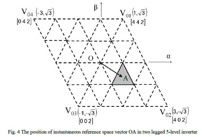 |
| The method of sector identification in the proposed work can be explained by considering a position of reference
space vector OA for a two legged 5-level inverter as in Fig. 4. In order to identify the sector, first determine the
location of the tip of the reference space vector OA from among the two regions of the equivalent 2-level inverter. In
the previous sections, it is mentioned that the switching voltage representation of 2-level inverter contains two sectors
(equilateral triangles) as a results of four voltage space vectors located at V01, V02, V03 and V04. α and β coordinates of
V01, V02, V03 and V04 for equivalent 2-level inverter are (1, √3), (3, -√3), (-1, -√3) and (-3, √3) as shown in Fig. 5(a).
The switching states of V01, V02, V03 and V04 are also shown in Fig. 5(a) [in square brackets]. To identify the sector
which encloses the tip of the reference space vector, compute the coordinates of the centroid of the both two equilateral
triangles of the equivalent 2-level inverter and found the triangle with centroid closest to tip of reference voltage space
vector. The coordinates of the centroid of the triangles can be determined by taking the average of the coordinates of the three vertices. In this case, it is found that ΔV01V02V03 is the triangular sector in which tip of the reference space
vector lies as shown in Fig. 5(a). The number of applications of triangularization algorithm for a 5-level inverter is two
[10]. In the first application of triangularization algorithm to the region [ΔV01V02V03] which encloses the tip of the
reference space vector, it gets divided into four equilateral triangles. Sector I of the equivalent 2-level inverter in which
tip of the reference space vector lies undergoes first triangularization algorithm and generate three additional vectors
V00, V11, V12 and gets divided in to four smaller triangular regions as in Fig. 5(b). |
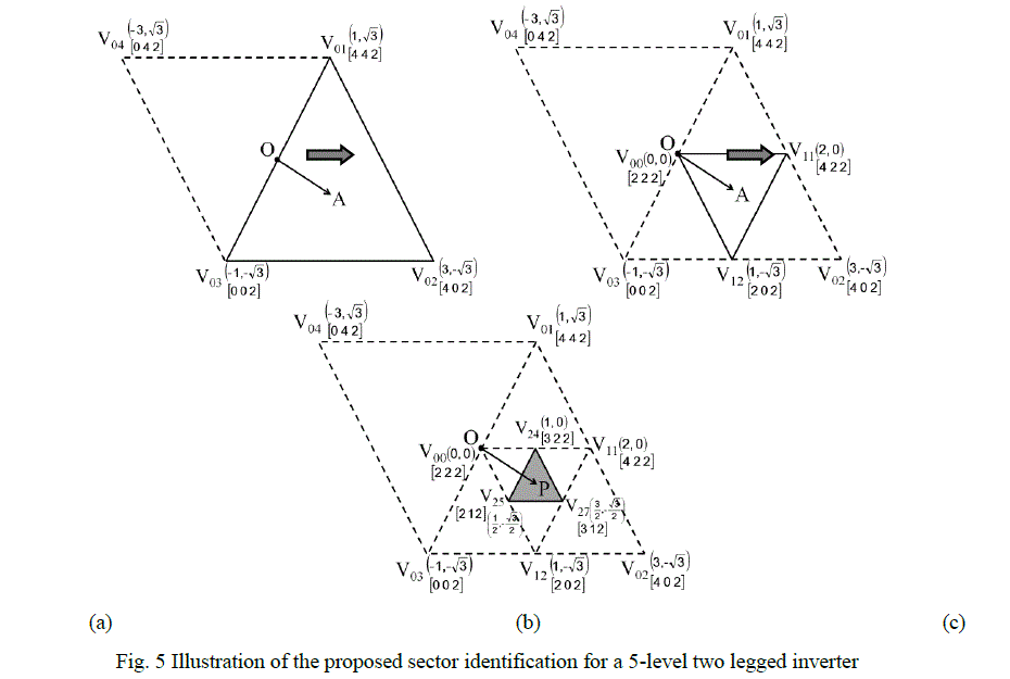 |
| According to Triangularization algorithm, the average of α and β coordinates of the voltage vectors at V01 and V02
will result in the coordinates of V11 as (2, 0). The averaging applied to the switching states at V01 and V02 will result in
the switching states corresponding to the switching vector located at V11 as [4 2 2]. The voltage vectors and switching
states of V12 and V00 are also computed similarly and are also shown in Fig. 5(b).Then again compute the centroid of
the new four triangular sectors and from among these sectors find the region in which the tip of the reference space
vector lies. It is found that the triangle which encloses the tip of the reference space vector OA is ΔV00V11V12. |
| For a 5-level inverter, the triangularization algorithm has to be applied once more. The application of
triangularization algorithm within the ΔV00V11V12 generate three additional vectors V24, V25, V27 and the corresponding
switching vectors and inverter states can be determined and are shown in Fig. 5(c). These three new vectors divide the
ΔV00V11V12 into four smaller triangles. From among these four triangles, determine the triangle in which the tip of the
reference space vector lies by computing the centroids. It is found that the ΔV24V25V27 encloses the tip of the reference
space vector and V24, V25 and V27 are the location of the switching vectors which are used to synthesize the reference
voltage space vector OA. This is the procedure for the sector identification and the switching vector determination. For
higher level inverters the procedure repeated to identify the sector and determine corresponding switching vector and
switching state of voltage space vectors. |
| B. Switching vector time calculations |
| The procedure for identification of sector and determination of switching voltage vectors are explained in the above
section. The next stage involves determining the duration for which the voltage space vectors located at the vertices of
the identified sector are to be switched. Since one phase is clamped to a constant voltage, space vector representation of
two legged multilevel inverter has unique zero vector. In the above case, the tip of the reference voltage space vector
OA is lies in the triangular sector formed by the voltage space vectors located at V24, V25 and V27. The coordinates of
the switching voltage space vectors located at V24, V25 and V27 are (1, 0), (1/2, -√3/2) and (3/2, -√3/2) as shown in Fig.
5(c). The switching time duration of the voltage vector is determined by using the volt-sec balancing principle [8].
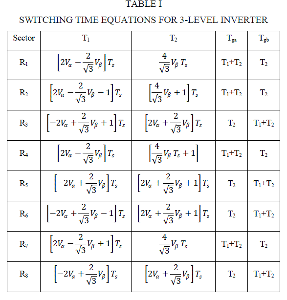
There is no mapping is used in the proposed work. The equations for switching time duration (T1 and T2) of the voltage
vectors for two legged 3-level inverter is given in Table I. The sampling time period for the space vector modulation is
denoted as Ts and it is equal to the sum of T1, T2 and T0. Hence the equation for T0 is obtained by, |
 |
| From the computed T0, T1 and T2, the inverter leg switching time for phase A and B (denoted as Tga and Tgb) are
computed as given in Table I. |
 |
SIMULATION RESULTS |
| To verify the validity of the proposed algorithm for generation of SVPWM, simulation is carried out in
MATLAB/SIMULINK for two legged three phase inverter fed Permanent Magnet Synchronous Motor (PMSM) drive
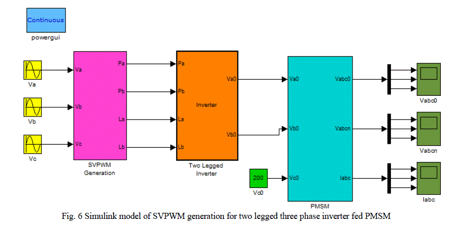
with a DC link voltage of 400V. Fig.6 shows the simulink model of SVPWM generation for two legged multilevel
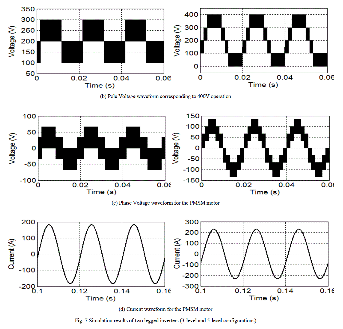
inverter fed PMSM. Fig. 7 presents the simulation results of two legged inverter for 3-level and 5-level operations with
phase C clamped to 200V. Tga represents the inverter leg switching time waveform and are shown in Fig. 7(a). Fig. 7(b)
shows the inverter pole voltage corresponding to 400V operation. For the 3-level operation (Va0) the inverter switches
between the levels of 150V, 200V and 250V. The levels of pole voltage for 5-level operations are 0V, 100V, 200V,
300V and 400V. The motor phase voltage and current are also shown in Fig. 7(c) and Fig. 7(d) respectively. |
| Simulation parameters are: |
| Fundamental frequency 50 Hz |
| Switching frequency 10 kHz |
| PMSM parameters: |
| Stator resistance, Rs 0.7 Ω |
| Stator inductance, Ls 2.72mH |
| Moment of inertia, J 0.0002 kg.m2 |
| Damping coefficient, B 0.002 N.m.s.rad-1 |
| Back-emf constant, Kb 0.5128 V/rad/sec |
| Rated speed, ωr 3000 rpm |
 |
 |
 |
CONCLUSION |
| This paper presents the fractal structure in the voltage representation of the two legged multilevel inverter and
utilizing the fractal structure the paper proposes a method for the SVPWM generation for the n-level two legged
inverter. The proposed work involves triangularization algorithm for the generation of the SVPWM and thus it simplify
the implementation process. No need of look up table for the sector identification. The basic unit of the fractal
structure of the two legged multilevel inverter is the triangle and each triangle is undergoes repeated division for higher level inverters. The implementation algorithm is explained for 5-level inverter and simulation results are presented for
3-level and 5-level inverter configurations. The proposed work can be easily extended for higher level two legged
inverters. |
References |
- J. S. Lai and F. Z. Peng, ―Multilevel converters–A new breed of power converters,IEEE Transactions on Industrial Applications, vol. 32, pp. 509–517, May/June1996.
- Jose Rodriguez, Jih-Sheng Lai and Fang ZhengPeng," Multilevel Inverters: A Survey of Topologies, Controls and Applications ", IEEE Transactions on Industrial Electronics, vol.49, No.4, August 2002, pp 724-738.
- H. W. van der Broeck and J. D. van Wyk, ―A comparative investigation of a three-phase induction machine drive with a component minimized voltage-fed inverter under different control options, IEEE Transactions on Industrial Applications, vol. IA-20, no. 2, pp. 309–320, Mar./Apr. 1984.
- J. Holtz, ―Pulse width modulation—A survey, IEEE Transactions on Industrial Electronics, vol. 39, no. 5, pp. 410–420, Dec. 1992.
- K. Zhou and D. Wang, ―Relationship between space-vector modulation and three-phase carrier-based PWM: A comprehensive analysis, IEEE Transactions on Industrial Electronics, vol. 49, no. 1, pp. 186–196, Feb. 2002.
- W. Yao, H. Hu, and Z. Lu, ―Comparisons of space-vector modulation and carrier based modulation of multilevel inverter,IEEE Transactions on Power Electronics, vol. 23, no. 1, pp. 45–51, Jan. 2008.
- B. P. McGrath and D. G. Holmes, ―Multi carrier PWM strategies for multilevel inverters,IEEE Transactions on Industrial Electronics, vol. 49, no. 4, pp. 858–867, Aug. 2002.
- H. W. V. D. Brocker, H. C. Skudenly and G. V. Stanke, ―Analysis and realization of a pulse width modulator based on the voltage space vectors, IEEE Transactions on Industrial Applications, vol. 24, no. 1, pp. 142-149, Jan./Feb. 1988.
- N. Celanovic and D. Boroyevich, ―A fast space-vector modulation algorithm for multilevel three-phase converters,IEEE Transactions on Industrial Applications, vol. 37, no. 2, pp. 637–641, Mar./Apr. 2001.
- AnishGopinath, Aneesh Mohamed A. S., and M. R. Baiju, ―Fractal based space vector PWM for multilevel inverters—A novel approach, IEEE Transactions on Industrial Electronics, vol. 56, no. 4, pp.1230–1237, Apr. 2009.
- Aneesh Mohamed A.S., AnishGopinath and M.R.Baiju, ―A simple space vector PWM generation scheme for any general n-level inverter, IEEE Transactions on Industrial Electronics, vol. 56, no. 5, pp.1649-1656, May 2009.
- C. B. Jacobina, E. R. C. da Silva, A. M. N. Lima, and R. L. A. Ribeiro, ―Vector and scalar control of a four switch three pha se inverter, in Proc. IEEE-IAS Annual Meeting, 1995, pp. 2422–2429.
- FredeBlaabjerg, SigurdurFreysson, H. Henrik Hansen and S. Hansen, ―A new optimized space vector modulation strategy for a component minimized voltage source inverter, IEEE Transactions on Power Electronics, vol. 12, No. 4, pp. 704-710, July 1997.
- M. B. R. Corrêa, C. B. Jacobina, E. R. C. Silva and A. M. N. Lima, ―A General PWM Strategy for Four-Switch three phase inverter, IEEE Transactions on Power Electronics, vol. 21, No. 6, pp.1618-1627, Nov. 2006.
- FredeBlaabjerg, Dorin O. Neacsu and John K. Pedersen, ―Adaptive SVM to Compensate DC-Link Voltage Ripple for Four-Switch Three- Phase, IEEE Trans. on Power Electronics, Vol. 14, No. 4, pp. 743-752, July 1999.
- Hong-Hee Lee, P.Q. Dzung, L.D. Khoa, L.M. Phuong, H.T. Thanh ―The Adaptive Space Vector PWM for Four Switch Three Phase Inverter Fed Induction Motor with DC– Link Voltage Imbalance, IEEE International Conference on Innovative Technologies for Societal Transformation- TENCON2008,Hyderabad, India, Nov. 18th -21st 2008.
- P.Q. Dzung, L.M. Phuong, P.Q. Vinh, N.M. Hoang, T.C. Binh, ―New Space Vector Control Approach for Four Switch Three Phase Inverter (FSTPI), International Conference on Power Electronics and Drive Systems- PEDS 2007, Bangkok, Thailand,2007
- H.O. Peitgen, H. Jurgens, and D. Saupe, Chaos and Fractals—New Frontiers of Science, 2nd ed. New York: Springer-Verlag, 2004.
|