Keywords
|
| Edge-Triggered D Flip-flop, Overlap Period , CMOS, C2MOS, PDN. |
INTRODUCTION
|
| CMOS technology has different logic styles to improve the performance of logic circuits and to get the most benefit of the new technologies. Crosstalk and Clock routing are the major issues in dynamic circuits. Digital circuits are designed to improve design metrics like reliability, power consumption, performance, and area. These approaches can be divided into static and dynamic logic styles. Dynamic circuits are superior in terms of speed and area compared to static circuits. |
| The conventional CMOS logic (static or dynamic) and pass transistor logic (PTL) [1] styles are two major architectures in implementing the logic circuits. The PTL family has been explored in the form of Transmission Gates (TGs), Complementary PTL (CPL), Double PTL (DPL), and Gate Diffusion Input (GDI) [2] logic styles. In some logic functions like multiplexers, the TG logic is more efficient compared to the static CMOS architectures. However, the TG circuits become very slow in a large set of cascaded functions due to the RC delay and body effects. The Gate Diffusion Input (GDI) technique, which is a kind of pass transistor logic (PTL) circuit, uses two-transistor cells to implement a logic function with reduced complexity. The voltage swing of the internal nodes is typically low which reduces the dynamic power consumption. However, it is not suitable for low voltage circuits and suffers from static power-consumption. All these structures are sensitive to the clock overlap. In order to get rid of the problem of clock overlap single clock DFFs are done. The DFFs in are also able to have negative setup times. A new structure for an overlap based DFF is proposed. This structure operates, to some extent, similar to the HLFF in, however, it achieves higher performance parameters compared to other DFFs. The acceptable overlap period in the proposed structure is much larger than other HLFFs [4]. This makes the design of such a DFF simpler. Also it is not necessary to accurately adjust the overlap time for each DFF in the circuit. |
CONVENTIONAL C2MOS DYNAMIC LOGIC
|
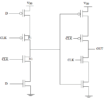
| In Dynamic C2MOS logic, there is not always a mechanism driving the output high or low. In the most common version of this concept, the output is driven high or low during distinct parts of the clock cycle. |
| Dynamic C2MOS logic requires a minimum clock rate fast enough that the output state of each dynamic gate is used before it leaks out of the capacitance holding that state, during the part of the clock cycle that the output is not being actively driven. |
| C2MOS logic, when properly designed, can be over twice as fast as static logic. It uses only the faster N transistors, which improve transistor sizing optimizations. Static logic is slower because it has twice the capacitive loading, higher thresholds, and uses slow P transistors for logic. Dynamic logic can be harder to work with, but it may be the only choice when increased processing speed is needed. |
THE PROPOSED OVERLAP BASED LOGIC CELL
|
| A. PROPOSED OVERLAP LOGIC CELL: |
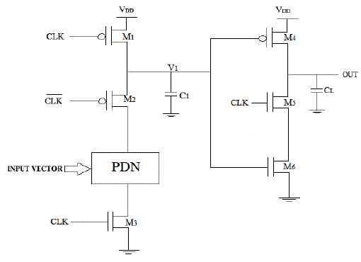
| The PDN(Pull-Down Network) network is replaced with single nmos to act as Simple DFF and the operation is explained as follows |
| B. BASIC OPERATION OF OVERLAP BASED LOGIC CELL: |
| The operation of the proposed logic cell can be divided into two modes as follows. |
| 1. Evaluation mode |
| 2. Holding mode |
| i. EVALUATION MODE |
| It happens only during 1–1 overlap of the clock signals. During this phase, transistors M2, M3, and M5 are all on. The second stage behaves like a simple inverter and the data can pass through the cell and reach the output where no delay in output occurs. This phase starts,V1 has been 0 and is at the beginning of this mode. |
| During this mode, the internal node V1 is disconnected from the input PDN,capacitor C1 holds the output from previous state and passes to the inverter while and can have the following values: |
| a) The 1–0 sequence ( clk and clk’ ): During this period, V1 has a value that is the inverse of the input PDN and has been stored during the evaluation mode. Moreover,V1 is inverted and passed to the output. |
| b) The 0–X sequence ( clk and clk’ ): Under this condition V1 is disconnected from both the input PDN and the output node and is pre-charged to Vdd . |
| The acceptable overlap range can be increased by the combinational delay between the logic cells. In this way, we did not add any combinational circuits between the two cells. This sequential logic is verified using cadence tool and acts as inverter with rise time and fall time delay of 10nS |
SIMULATION RESULTS
|
| The simulation results were obtained from Cadence in 180nm CMOS process at room temperature VDD is 1.8V. All flip flops were simulated with output load capacitance CL. |
| Total no of Transistors: The total number of transistors is measured which contribute more area and power consumption in the integrated circuit design. |
| Power: The total power consumption of Overlap flip flop in terms of μw (micro watt).the maximum power denotes the maximum power consumption of flip flop. The minimum power describe the minimum power requirement to trigger the flip flop |
| A. OVERLAP BASED DFF |
| The Overlap D-Flip-flop schematic was created using the Schematic editor in Cadence and was extracted for the logic simulation and the Power results are obtained for comparison. Table I summarizes some important performance indexes of these D-FF design. These include transistor count, and Average power. |
| B. OVERLAP LOGIC CELL D-FF POWER RESULT |
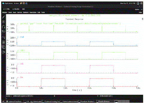
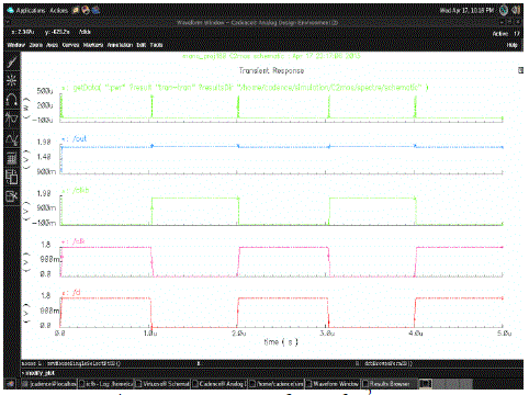
| Fig 4.2 illustrates the Transient power analysis waveform of Overlap based DFF. When at positive edge of clock ,CLK=1 and CLK’=1 ,the circuit works as DFF .D=1 and OUT=1 and in Fig 4.2(a) Power is obtained as 1.746 μw. |
| C. C2MOS POWER RESULTS: |
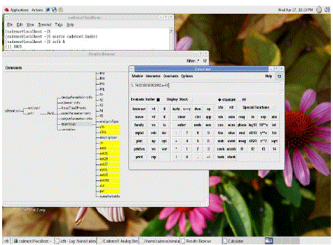
| Fig 4.3 illustrates the Transient power analysis waveform of C2MOS. When CLK=1 and CLK’=1 ,the circuit. D=1 and OUT=1 and in Fig 4.3(a) Power is obtained as 2.660μw. |
| D. OUTPUT ANALYSIS |
| The Transient Power analysis is done with Stop time of 5μS, Clk and its Complement Clkb has 10nS of delay time to make the operation happen at 1-1 overlap. |
CONCLUSION
|
| The Power reduction in Overlap DFF is due to usage of Overlap Period of the clock signals. Clock Overlapping concept is done by using this proposed Overlap based Logic cell. Number of transistors are reduced and power analysis is done, where low power is consumed by this proposed logic. Transient power analyses is obtained using cadence tool. Power gets reduced by 35% using overlap based D-FF which is more Power efficient. |
Tables at a glance
|
 |
| Table 1 |
|
Figures at a glance
|
 |
 |
 |
| Figure 1 |
Figure 2 |
Figure 3 |
 |
 |
 |
| Figure 4 |
Figure 5 |
Figure 6 |
|
References
|
- .OmidSarbishei and Mohammad Maymandi-Nejad, Member, IEEE,” A Novel Overlap-Based Logic Cell: An Efficient mplementation of Flip–Flops With Embedded Logic” IEEE Transactions on very large scale integration (vlsi) systems. Vol. 18, no. 2, february 2010.
- .Morgenstein, A. Fish, and I. A. Wagner, âÃâ¬Ãâ¢Gate-diffusion input (GDI)—A power efficient method for digital combinatorial circuits,âÃâ¬ÃâIEEETrans. Very Large Scale Integr. (VLSI) Syst., vol. 10, no. 5, pp. 566–581, Oct. 2002.
- .Morgenshtein, A. Fish, and I. A. Wagner, âÃâ¬Ãâ¢An efficient implementation of D-flip–flop using the GDI technique,âÃâ¬Ãâ in Proc. Int. Symp.Circuits Syst. (ISCAS 2004), May , vol. 2, pp. II-673–II-676.
- O. Sarbishei and M. Maymandi-Nejad, âÃâ¬Ãâ¢Power-delay efficient overlapbased charge-sharing free pseudo-dynamicD flip–flops,âÃâ¬Ãâ in Proc.IEEE ISCAS, 2007, pp. 637–640.
- H. Partovi, R. Burd, U. Salim, F.Weber, L. DiGregorio, and D. Draper, Flow-through latch and edge-triggered flip–flop hybrid elements,âÃâ¬Ãâ in IEEE ISSCC Dig. Tech. Papers, 1996, pp. 138–139.
- W. L. Goh, âÃâ¬Ãâ¢Delay sensitivity study on process, supply voltage and temperature variations of single edge-triggered flip–flops,âÃâ¬Ãâ in Proc.Symp. Low-Power High-Speed Chips, Apr. 2007, pp. 151–162.
- X. Cheng and R. Duane, âÃâ¬Ãâ¢0.6 V D flip–flop utilising negative differential resistance device,âÃâ¬ÃâElectron. Lett., vol. 42, no. 7, pp. 388–390, Mar.2006.
- J. Yuan and C. Svensson, âÃâ¬Ãâ¢New single-clock CMOS latches and flip flops with improved speed and power savings,âÃâ¬ÃâIEEE J. Solid-StateCircuits, vol. 32, no. 1, pp. 62–69, Jan. 1997.
- V. Stojanovic and V. G. Oklobdzija, âÃâ¬Ãâ¢Comparative analysis of master–slave latches and flip–flops for high-performance and low-power systems,âÃâ¬Ãâ IEEE J. Solid-State Circuits, vol. 34, no. 4, pp.536–548, Apr. 1999.
- X. Cheng and R. Duane, âÃâ¬Ãâ¢0.6 V D flip–flop utilising negative differential resistance device,âÃâ¬ÃâElectron. Lett., vol. 42, no. 7, pp. 388–390, Mar. 2006.
- P. M.Wai, âÃâ¬Ãâ¢High-performance output feedback flip–flop for ultra low power applications,âÃâ¬ÃâInt. J. Electr. Eng., vol. 13, no. 1, pp. 29–39, Feb.2006.
- V. Tirumalashetty and H. Mahmoodi, âÃâ¬Ãâ¢Clock gating and negative edge triggering for energy recovery clock,âÃâ¬Ãâ in Proc. IEEE ISCAS, 2007, pp.1141–1144.
- W. L. Goh, âÃâ¬Ãâ¢Delay sensitivity study on process, supply voltage and temperature variations of single edge-triggered flip–flops,âÃâ¬Ãâ in Proc.Symp. Low-Power High-Speed Chips, Apr. 2007, pp. 151–162.
|