INTRODUCTION
|
| An adaptable system which is capable of responding to a wide range input voltage and current conditions is required by more conventional dc-dc converter configuration as it is opposed to power conversion for photo voltaic application. The variation in panel construction and operating temperature makes the PV voltage to vary significantly. Solar irradiance and shading conditions will change the PV current to a large extent. As the range of conditions relating to many PV installations will make the converter to operate in another region which will be the less efficient one if the converter is designed only for a high peak efficiency. |
| The galvanic isolation between the PV panel and the electric utility system is the necessity design process of PV PCS. Due to various reasons the galvanic isolation is preferred. The main benefits among these are improved voltage boost ratio, reduced ground leakage current, and over all safety improvement during fault condition. |
| The distributed maximum power point will achieve better energy production. The PV panels connected in parallel will be more productive in light load and partially shaded conditions than a series connected system. |
| On the view of the above reason the isolated micro converter (dc-dc), a best option from a performance based analysis. This attempts to regulate the dc-link voltage by sending power to utility grid. |
| The isolated dc-dc stage have to be operated efficiently at high power, and also to maintain high performance at light load, across a wide ranges of PV voltages in a distributed PV PCS. It is able to reduce the amount of circulating current in the circuit in order to maintain the high efficiency under low power conditions. |
| A well known option for dc-dc conversion stage is a simple continuous conduction mode (CCM) fly back converter. The simple construction and circulating are the most advantages. But the overall system efficiency will be typically low (< 90%) due to the switching loss for both diode and the primary switch is quite large. The another option is series resonant converter and more recently the LLC resonant converter, they both operate on a similar principle and use a variable frequency control to adjust the output voltage. The series resonant converter when operated near the resonant frequency the converter reaches nearly ZVS and zero-current switching (ZCS) with a low circulating energy giving high peak efficiency. During the operation however, the circuit frequency diverges from the resonant frequency which leads to the increase in the circulating current and finally reduces over all system efficiency. |
| Beyond these two options we are also having another method by which we can regulate over a wide input range with no switching loss or no circulating energy, very high peak efficiency, and integrated isolation by the use of series-resonant converter as an regulated dc-dc transformer. |
| The method of using the series resonant dc-dc transformer is best one, but the system requires an additional element to provide regulation capability. In this proposed method we are using only a single inductor as an additional element to the circuit. The circuit is straight forward in operation and uses multiple PWM to observe minimum and maximum duty cycle. |
PROPOSED CIRCUIT
|
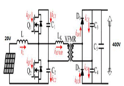
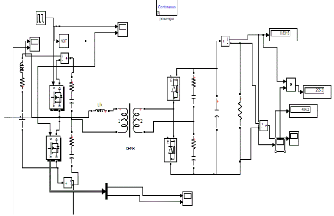
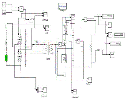
| In this proposed boost converter operation is implemented by the two MOSFET. The inductor directly connects to the mid points of the both active switching legs simultaneously this will make a connection with the one terminal of the transformer. The two MOSFETs Q1 and Q2 will be in parallel until their patterns of switching are synchronised. In this circuit topology the output diodes D1 and D2 will achieve ZCS until the resonant behaviour is allowed to complete. |
| For integrated boost resonant control implementations that are possible are input voltage, input current and direct duty cycle control which gives a flexible control. There will be four different operating modes of the proposed circuit and also provided their timing diagram: |
| MODE 1[to<t<t1]: |
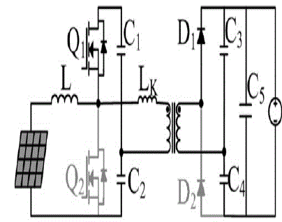
| In this mode Q1 will get into ON condition by ZVS condition at t0.The capacitor C1 will be in the resonating with the transformer leakage inductance and the capacitor on the output side through D1.The difference of transformer current flowing through C1 through the positive terminal of transformer and the input current. |
| MODE 2[t1<,t<t2]: |
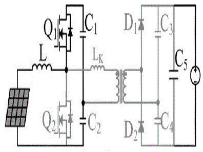
| Q1 will be in ON condition conducting only the input inductor current, which continuous to decrease. The resonant elements will be in zero current and at end of this mode the Q1 will get into OFF which will make Q2 to ON. |
| MODE 3[t2<t<t3]: |
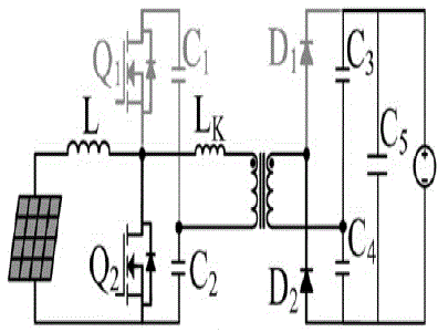
| In this mode C2 begins to resonate with transformer leakage current having a parallel combination of C3 and C4 through the diode D2.So, the inductor current increases linearly. The Q2 carries sum of the transformer current and the inductor current. |
| MODE 4[t3<t<t4]: |
| The Q2 will get into OFF condition by the continuous flow of inductor current to the lower devices. |
RESULTS
|
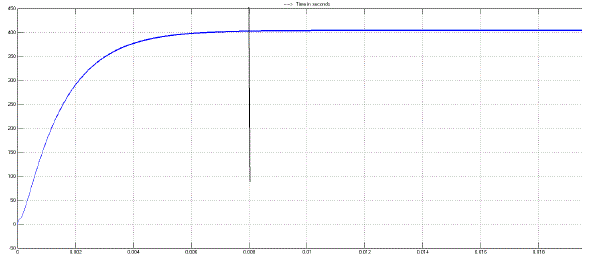
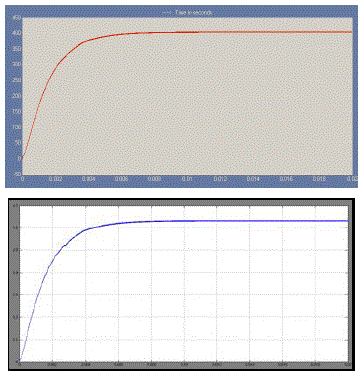
| A .SIMULATION OF THE PROPOSED IBR .OPEN LOOP CONVERTER |
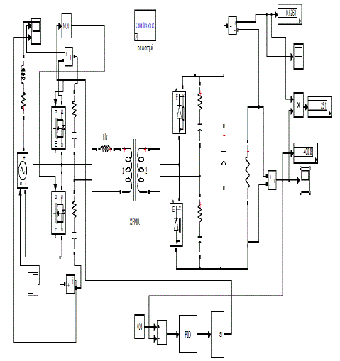
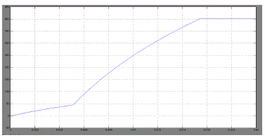
| B .SIMULATION OF THE PROPOSED IBR CLOSED LOOP CONVERTER |
| C .SIMULATION OF THE PROPOSED IBR CONVERTER WITH MPPT TECHNIQUE |
CONCLUSION
|
| The proposed circuit topology provided a good efficiency over a wide range of inputs, maintaining a very low switching losses and circulating current. As the circuit is of a simple construction it costs very low and also the control of the circuit is simple process which only have to maintain the resonant period with the duty cycle range. |
Figures at a glance
|
tr>
 |
 |
 |
 |
 |
| Figure 1 |
Figure 2 |
Figure 3 |
Figure 4 |
Figure 5 |
 |
 |
 |
 |
 |
| Figure 6 |
Figure 7 |
Figure 8 |
Figure 9 |
Figure 10 |
|
References
|
- E. Roman, R Alonso, P. Ibanez, S. Elorduizapatarietxe, and D. Goitia, “Intelligent PV module for grid-connected PV system,” IEEE Trans.Ind.Electron., vol. 53, no. 4,pp. 1066-1073,jun. 2006
- Y. C. Hsieh, M. R. Chen, and H. L. Cheng, “An interleaved flyback converter featured with zero-voltage transition,” IEEE Trans. Power Electron., vol. 26, no. 11, pp. 3205-3214, Nov. 2011.
- G. Spiazzi, P. Mattavelli, and A. Costabeber, “High step-up ratio flyback converter with active clamp and voltage multiplier,” IEE Trans. Power Electron., vol. 26, no. 11, pp. 3205-3214, Nov. 2011.
- Y. Gu, L. Hang,Z. Lu, Z. Qian, and D. Xu, “Voltage doubler application in isolated resonant converters,” in proc. Ind. Electron. Soc., 2005, p.5.
- J. F. Lazar and R. Martinelli, “Steady-state analysis of the LLC series resonant converter,” in Proc. Appl. Power Electron. Conf., 2001, vol. 2, pp. 728-735.
|