Keywords
|
| FPGA, MicroBlaze, Virtex-5, EDK, XPS, SDK, lwIP. |
INTRODUCTION
|
| The reconfigurable devices, such as FPGA are flexible and reusable high-density circuits. That is, any portion of the system can be reconfigured at any time while the rest of the design is still working. With the advancement of Field Programmable Gate Arrays (FPGAs) a new trend of implementing the microprocessors on the FPGAs has emerged in the design community [1]. The design of such microprocessors is available in the form of software bitstream, so they are called soft-processors or soft cores. System designers can embed these cores into their designs and have the option to customize them as required. Soft cores are technology independent and require only simulation and timing verification. This reduces the design time as compared to a hard core processor. |
| In Ethernet communication the data will be secured with a header, so there requires a method that can be used to retrieve actual data from the Ethernet data. If a processor is used, this can be done quite easily with good speed and also the actual data can be further processed as required. While a processor based system could simplify data retrieval and processing, the processor embedded inside the system simplifies the technique further since it requires only less number of components thereby reducing the device utilization. So all these factors prompted us to implement a system using an embedded processor that receives Ethernet packets, retrieve actual data, modify it and finally transmit it to any other destinations required with the help of Embedded Development Kit. The implementation platform is the ML505 board which supports the embedded processor MicroBlaze. MicroBlaze is a 32-bit RISC Harvard architecture soft processor IP core with a rich instruction set optimized for embedded applications [2]. The implementation is achieved using the Embedded Development Kit provided by Xilinx, which helps to design the complete embedded processor more quickly and easily [3]. |
SOFTWARE OVERVIEW
|
| Embedded Development Kit (EDK) is an integrated software tool for developing embedded systems [4]. The EDK package has Xilinx Platform Studio (XPS) software for configuring the hardware portion and Software Development Kit (SDK) for configuring the software portion. XPS includes a graphical user interface that provides a set of tools to help in the project design. The Base System Builder (BSB) is a wizard in the XPS that quickly and efficiently establishes a working design, which can then be customized by the designer. XPS supports the creation of the Microprocessor Hardware Specification (MHS) and Microprocessor Software Specification (MSS) files needed for embedded tools flow. The MHS file defines the system architecture, peripherals and embedded processors [5]. The software platform is defined by MSS file which defines driver and library customization. |
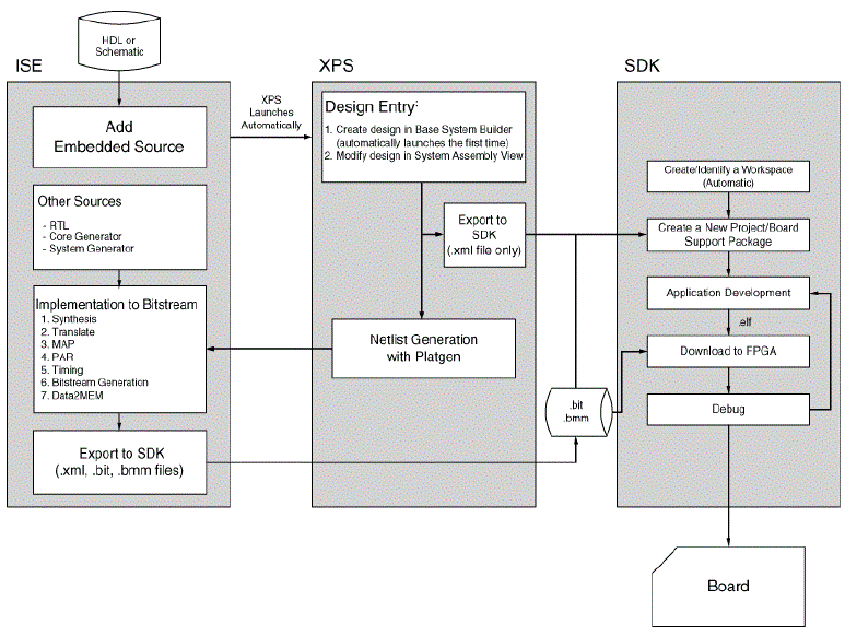
| After designing the hardware portion, the design has to undergo different processes like Synthesis, Simulation, Translate, Map and Place and Route. Finally, a bit file is generated. This bit file is exported to the SDK along with the MHS and MSS files. SDK is an integrated development environment, complimentary to XPS. It can create different software applications for peripherals and processors that have been connected in XPS. The code can be written in the high level programming language C/C++. The block diagram that represents the basic embedded design flow can be seen in Fig. 1[3]. |
SYSTEM DESIGN
|
| The implementation platform is the ML505 evaluation board that have Virtex-5 FPGA. The ML505 board support MicroBlaze soft core processor. The system design is divided into two. One is hardware design, which includes the designing methods using XPS and the other is Software design, which include designing methods using SDK. |
| A. Hardware Design |
| Besides the MicroBlaze, other components required by the design are GPIO LEDs, a timer, an interrupt handling controller and a serial communication device UART. The MicroBlaze is implemented entirely in the general-purpose memory and logic fabric of FPGAs using the EDK design environment. The BSB (Base System Builder) Wizard inside XPS is used for generating the embedded system around the MicroBlaze that is supported on the ML505 board. This wizard allows the selection of the board and processor. |
| As a first step, the MicroBlaze processor is configured. Here we set the system clock frequency to 125 MHz and the local memory to 64 KB. The next step is the selection and configuration of peripherals, which include the DDR_SDRAM memory, the serial communication device RS232_UART, GPIO LEDs for display, Hard Ethernet MAC – ‘xps_ll_temac’ and timer - ‘xps_timer’. The timer was used for the reference time generation part. |
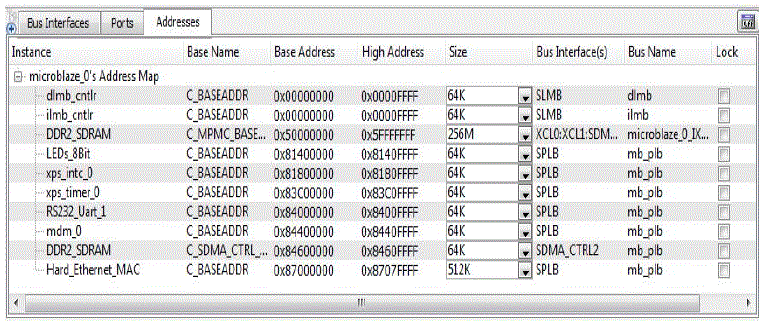
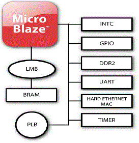
| Interrupt is enabled for both Hard Ethernet MAC and the timer. Interrupt handling was done with the help of the interrupt handling controller (INTC) named xps_intc_0. The instruction and data cache configuration is the final part. The automatically generated addresses by the XPS tool for each IP cores are shown in Fig. 2. The resulted block diagram of the design is shown in Fig. 3 [6]. |
| B. Software Design |
| The software part of the design is configured using the SDK tool. For configuring the software portion we have to export the hardware design to the SDK along with the BIT file. SDK provides us with a great number of project templates that we can pick from. In our design we have to configure the Ethernet MAC inside the ML505 board such that it can receive UDP packets. So to meet our requirement, we can select the lwIP Echo Server template from the available templates [7]. The lwIP Echo Server template provides a simple demonstration of how to use the light weight IP stack. The server works on TCP data and listen for the input at the specified port and simply echoes back whatever data is sent to that port. Our requirement is to receive UDP packets, modify them and either transmit them or else display them on the LEDs. So we developed our C-program accordingly. In our design we will bind the IP address 192.168.1.10 with our board’s MAC address. Also our design is configured such that it will be listening for the input at the port 1234. |
IMPLEMENTATION
|
| The FPGA board is connected to an Ethernet port on the host computer via an Ethernet cable. Next an IP address is assigned to the Ethernet interface on the host computer. The IP address of the PC and the board must be in the same subnet. The software application assigns a default IP address of 192.168.1.10 to the board. So in our design we are assigning the PC with the IP address 192.168.1.100. |
| The C-code written in SDK is compiled with the GNU Compiler tool. The compiled C-files along with the libraries generate the executable Executable and Linkable File (ELF) file. The final stage of designing is the association between the hardware and software parts and the download of the entire image into the FPGA. For this we will use the Data2MEM tool which links the BIT (bitstream) file generated at the end of hardware implementation and the compiled ELF file. The result is a download.bit file and this is downloaded into the FPGA. After successful download, we will get the output shown in Fig. 4 at the serial port. |
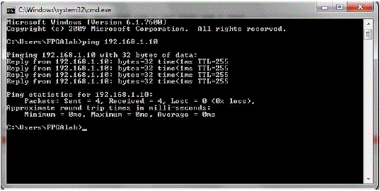
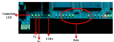
| Now we will be able to ping to the IP address 192.168.1.10 from the PC. The ping result can be seen in the Fig. 5. We use a LabVIEW program which can transmit UDP packets to the IP address 192.168.1.10. So as we run the LabVIEW program we can see that the Ethernet LED’s in the ML505 board lights up indicating that Ethernet reception and transmission are in progress. The Ethernet connection LED, transmission LED and reception LED lights up along with the reception and transmission speed indicator LED indicating 1 Gbps operation. If we have interfaced the design with the GPIO LEDs, we can see the result on LEDs. In the Fig. 6, you can see the data “1D” displayed on the GPIO LEDs. |
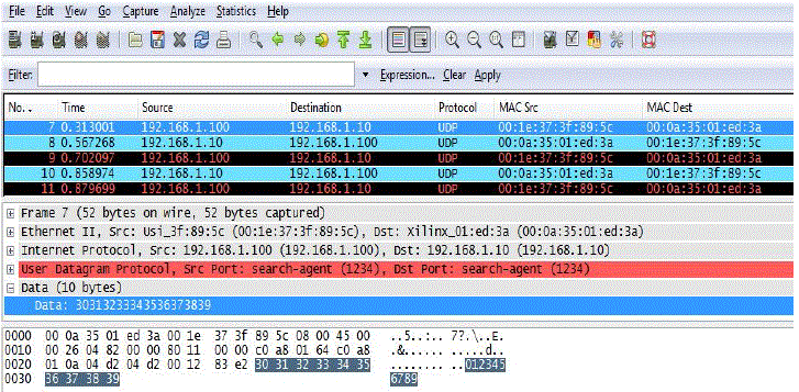
| To verify that the frames are correctly received and transmitted, the frames are captured using Wireshark. From the packets captured using Wireshark (see Fig. 7), it is noted that the packets that are transmitted from the PC using the LabVIEW program are received on the board. The data that are transmitted are 1, 2, 3, 4, 5, 6, 7, 8 and 9. By checking the data field of the received packet, we have seen that the ASCII values of the data are received on the board. That is, 31, 32, 33, 34, 35, 36, 37, 38 and 39. |
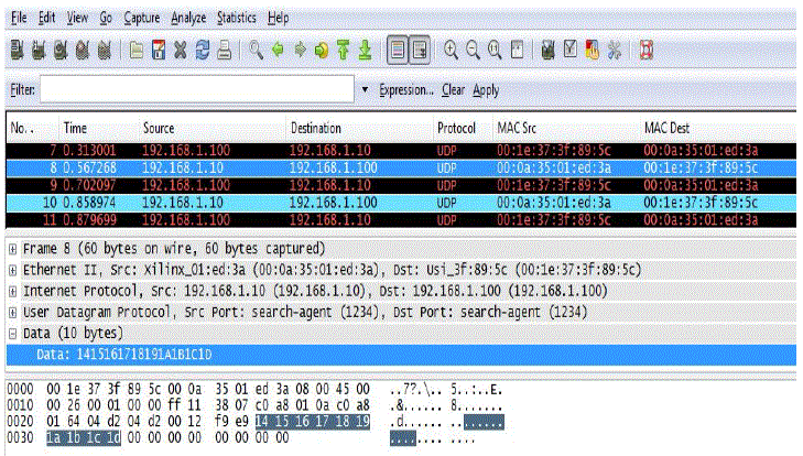
| In the present case, the modifications include converting the data in ASCII format into the corresponding decimal format, adding a constant decimal value “20” to them and then transmit them back to the PC. In Fig. 8, we can see the corresponding hex values of the modified data are transmitted back to the PC. That is, 14, 15, 16, 17, 18, 19, 1A, 1B, 1C and 1D. |
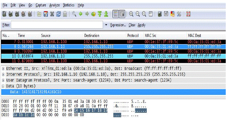
| We are able to transmit the data to any IP address by making required changes in the corresponding C file. In the Wireshark result shown in Fig. 9, it can be seen that the board is receiving data from the IP address 192.168.1.100 and after modifying the received data, it is broadcasted. |
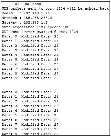
| If we are trying to display the modified data by adding suitable print commands in the main C-file, we will get the output shown in Fig. 10, at the serial port. |
CONCLUSION
|
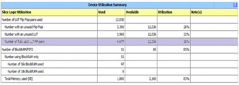
| MicroBlaze processor with Hard Ethernet MAC was configured using the EDK tool. Using SDK, lwIP was configured inside the processor. The configuration is capable of receiving packets sent to the board’s IP address. The processor will modify the data accordingly and will display it on the LEDs. We were also able to transmit the modified data to any IP address required. The details of FPGA resource utilization is given in Fig. 11. |
ACKNOWLEDGMENTS
|
| The authors wish to thank Director, NPOL for permitting to carry out this project. Authors also wish to thank Mr. Suresh M., Scientist G, NPOL and Mrs. Jayamma T. M., Scientist F, NPOL for their valuable guidance, help and insightful comments. |
Figures at a glance
|
 |
 |
 |
 |
| Figure 1 |
Figure 2 |
Figure 3 |
Figure 4 |
 |
 |
 |
 |
| Figure 5 |
Figure 6 |
Figure 7 |
Figure 8 |
 |
 |
 |
| Figure 9 |
Figure 10 |
Figure 11 |
|
References
|
- Xilinx Inc. MicroBlaze Reference Manual, UG081 (v13.2)
- Xilinx,http://www.xilinx.comlproducts/design
- EDK Concepts, Tools and Techniques, A Hands-On Guide to Effective Embedded System Design, UG683 April 24, 2012
- Embedded System Tools Guide, October 6, 2003
- Platform Specification Format Reference Manual, UG642 July 6, 2011
- ml505_overview_setup
- Xilinx, Embedded System Example, XAPP1026, version 2.2, 2006
- National Instruments LabVIEW Fundamentals and Getting Started Guide.
|