Keywords
|
| Coupled inductor, high-efficiency power conversion, single-input multiple-output (SIMO) converter, Soft Switching, voltage clamping. |
| |
| |
INTRODUCTION
|
| In Order to protect the natural environment on the earth, the development of clean energy without pollution has the major representative role in the last decade . By dealing with the issue of global warming, clean energies, such as fuel cell (FC), photovoltaic, and wind energy, etc., have been rapidly promoted. Due to the electric characteristics of clean energy, the generated power is critically affected by the climate or has slow transient responses, and the output voltage is easily influenced by load variations . Besides, other auxiliary components, e.g., storage elements, control boards, etc., are usually required to ensure the proper operation of clean energy. For example, an FC-generation system is one of the most efficient and effective solutions to the environmental pollution problem. In addition to the FC stack itself, some other auxiliary components, such as the balance of plant (BOP) including an electronic control board, an air compressor, and a cooling fan, are required for the normal work of an FC generation system. |
| In other words, the generated power of the FC stack also should satisfy the power demand for the BOP. Thus, various voltage levels should be required in the power converter of an FC generation system. In general, various singleinput single-output dc–dc converters with different voltage gains are combined to satisfy the requirement of various voltage levels, so that its system control is more complicated and the corresponding cost is more expensive. The motivation of this study is to design a single-input multiple-output (SIMO) converter for increasing the conversion efficiency and voltage gain, reducing the control complexity, and saving the manufacturing cost. Patra et al. presented a SIMO dc–dc converter capable of generating buck, boost, and inverted outputs simultaneously. However, over three switches for one output were required. This scheme is only suitable for the low output voltage and power application, and its power conversion is degenerated due to the operation of hard switching. Nami et al. proposed a new dc–dc multi-output boost converter, which can share its total output between different series of output voltages for low- and high-power applications. Unfortunately, over two switches for one output were required, and its control scheme was complicated. Besides, the corresponding output power cannot supply for individual loads independently. Chen et al. investigated a multiple-output dc–dc converter with shared zero-current switching (ZCS) lagging leg. |
| In this paper,converter with the soft-switching property can reduce the switching losses, this combination scheme with three full-bridge converters is more complicated, so that the objective of high-efficiency power conversion is difficult to achieve, and its cost is inevitably increased. This study presents a newly designed SIMO converter with a coupled inductor. The proposed converter uses one power switch to achieve the objectives of high-efficiency power conversion, high step-up ratio, and different output voltage levels. In the proposed SIMO converter, the techniques of soft switching and voltage clamping are adopted to reduce the switching and conduction losses via the utilization of a low-voltage-rated power switch with a small RDS(on). Because the slew rate of the current change in the coupled inductor can be restricted by the leakage inductor, the current transition time enables the power switch to turn ON with the ZCS property easily, and the effect of the leakage inductor can alleviate the losses caused by the reverse-recovery current. Additionally, the problems of the stray inductance energy and reverse-recovery currents within diodes in the conventional boost converter also can be solved, so that the high-efficiency power conversion can be achieved. The voltages of middle-voltage output terminals can be appropriately adjusted by the design of auxiliary inductors; the output voltage of the high-voltage dc bus can be stably controlled by a simple proportional-integral (PI) control. |
II.CONVERTER DESIGN AND ANALYSIS
|
| The system configuration of the proposed high-efficiency SIMO converter topology to generate two different voltage levels from a single-input power source is depicted in circuit diagram. This SIMO converter contains five parts including a low-voltage-side circuit (LVSC), a clamped circuit, a middle-voltage circuit, an auxiliary circuit, and a high-voltage-side circuit (HVSC). The major symbol representations are summarized as follows. VFC (iFC) and VO1 (iO1 ) denote the voltages (currents) of the input power source and the output load at the LVSC and the auxiliary circuit, respectively; VO2 and iO2 are the output voltage and current in the HVSC. CFC, CO1 , and CO2 are the filter capacitors at the LVSC, the auxiliary circuit, and the HVSC, respectively; C1 and C2 are the clamped and middlevoltage capacitors in the clamped and middle-voltage circuits, respectively. LP and LS represent individual inductors in the primary and secondary sides of the coupled inductor Tr, respectively, where the primary side is connected to the input power source; Laux is the auxiliary circuit inductor. |
| The main switch is expressed as S1 in the LVSC; the equivalent load in the auxiliary circuit is represented as RO 1 , and the output load is represented as RO 2 in the HVSC. The corresponding equivalent circuit given in equivalent circuit is used to define the voltage polarities and current directions. The coupled inductor in system configuration can be modeled as an ideal transformer including the magnetizing inductor Lmp and the leakage inductor Lkp in equivalent circuit. |
| N1 and N2 are the winding turns in the primary and secondary sides of the coupled inductor Tr . Because the voltage gain is less sensitive to the coupling coefficient and the clamped capacitor C1 is appropriately selected to completely absorb the leakage inductor energy , the coupling coefficient could be simply set at one (k = 1) to obtain Lmp = LP . In this study, the following assumptions are made to simplify the converter analyses: 1) The main switch including its body diode is assumed to be an ideal switching element; and 2) The conduction voltage drops of the switch and diodes are neglected. |
This converter operates in six modes of operation:
|
| Mode 1 (t0 –t1 ): In this mode, the main switch S1 was turned ON for a span, and the diode D4 turned OFF. Because the polarity of the windings of the coupled inductor Tr is positive, the diode D3 turns ON. The secondary current iLs reverses and charges to the middle voltage capacitor C2 . When the auxiliary inductor Laux releases its stored energy completely, and the diode D2 turns OFF, this mode ends. |
| Mode 2 (t1 –t2 ) : At time t = t1 , the main switch S1 is persistently turned ON. Because the primary inductor LP is charged by the input power source, the magnetizing current iLmp increases gradually in an approximately linear way. At the same time, the secondary voltage vLs charges the middle-voltage capacitorC2 through the diode D3 . Although the voltage vLmp is equal to the input voltage VFC both at modes 1 and 2, the ascendant slope of the leakage current of the coupled inductor (diLkp /dt) at modes 1 and 2 is different due to the path of the auxiliary circuit. Because the auxiliary inductor Laux releases its stored energy completely, and the diode D2 turns OFF at the end of mode 1, it results in the reduction of diLkp /dt at mode 2. |
| Mode 3 (t2 –t3 ) : At time t = t2 , the main switch S1 is turned OFF. When the leakage energy still released from the secondary side of the coupled inductor, the diode D3 persistently conducts and releases the leakage energy to the middle-voltage capacitor C2 . When the voltage across the main switch vS 1 is higher than the voltage across the clamped capacitor VC 1 , the diode D1 conducts to transmit the energy of the primary-side leakage inductor Lkp into the clamped capacitor C1 . At the same time, partial energy of the primary-side leakage inductor Lkp is transmitted to the auxiliary inductor Laux, and the diode D2 conducts. Thus, the current iL aux passes through the diode D2 to supply the power for the output load in the auxiliary circuit. When the secondary side of the coupled inductor releases its leakage energy completely, and the diode D3 turns OFF, this mode ends. |
| Mode 4 (t3 –t4 ) : At time t = t3 , the main switch S1 is persistently turned OFF. When the leakage energy has released from the primary side of the coupled inductor, the secondary current iLS is induced in reverse from the energy of the magnetizing inductor Lmp through the ideal transformer, and flows through the diode D4 to the HVSC. At the same time, partial energy of the primaryside leakage inductor Lkp is still persistently transmitted to the auxiliary inductor Laux, and the diode D2 keeps to conduct. Moreover, the current iL aux passes through the diode D2 to supply the power for the output load in the auxiliary circuit. |
| Mode 5 (t4 –t5 ) : At time t = t4 , the main switch S1 is persistently turned OFF, and the clamped diode D1 turns OFF because the primary leakage current iLkp equals to the auxiliary inductor current iL aux. In this mode, the input power source, the primary winding of the coupled inductor Tr , and the auxiliary inductor Laux connect in series to supply the power for the output load in the auxiliary circuit through the diode D2 . At the same time, the input power source, the secondary winding of the coupled inductor Tr , the clamped capacitor C1 , and the middle voltage capacitor (C2 ) connect in series to release the energy into the HVSC through the diode D4 . |
| Mode 6 (t5 –t6 ) : At time t=t5 , this mode begins when the main switch S1 is triggered. The auxiliary inductor current iL aux needs time to decay to zero, the diode D2 persistently conducts. In this mode, the input power source, the clamped capacitor C1 , the secondary winding of the coupled inductor Tr , and the middle-voltage capacitor C2 still connect in series to release the energy into the HVSC through the diodeD4 . Since the clamped diodeD1 can be selected as a low-voltage Schottky diode, it will be cut off promptly without a reverse-recovery current. Moreover, the rising rate of the primary current iLkp is limited by the primary-side leakage inductor Lkp . Thus, one cannot derive any currents from the paths of the HVSC, the middle-voltage circuit, the auxiliary circuit, and the clamped circuit. As a result, the main switch S1 is turned ON under the condition of ZCS and this soft-switching property is helpful for alleviating the switching loss. When the secondary current iLS decays to zero, this mode ends. After that, it begins the next switching cycle and repeats the operation in mode 1. |
| This circuit shows the simulation model of Improved DC-DC to (SIMO) converter. Which contains one power switch(MOSFET),four diodes,and two loads namely Auxilary load and HVSC load, and all are connected by one scope to see the outputs. |
V.RESULTS
|
| The Figures 1&2 shows the experimental results of input voltage source and input current source respectively.And the graph is plot between time period vs voltage in volts and current in ampears.And the results are shown below. |
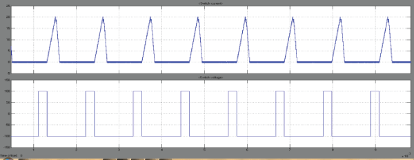
| The Fig3 shows the simulation output of switch(MOSFET)current and voltages. The graph plot between timeperiod vs current and voltages. And the results are shown below. |
| The Figures 4 &5 shows the simulation outputs of diode1 current &voltage and diode2 current and voltage respectively.The graph plot between timeperiod vs current and voltages. The results are shown below. |
| The Figures 6 &7 shows the simulation outputs of diode3 current &voltage and diode4 current and voltage respectively.The graph plot between timeperiod vs current and voltages. The results are shown below. |
| The Figures 8&9 shows the experimental results of output voltage at auxiliary load and HVSC loads respectively.And the graph is plot between time period vs voltage in volts.And the results are shown below. |
VI.CONCLUSION
|
| This topology adopts only one power switch to achieve the objective of high-efficiency SIMO power conversion. The voltage gain can be substantially increased by using a coupled inductor.The stray energy can be recycled by a clamped capacitor into the auxiliary battery module or high-voltage dc bus to ensure the property of voltage clamping .An auxiliary inductor is designed for providing the charge power to the auxiliary battery module and assisting the switch turned ON under the condition of ZCS. The switch voltage stress is not related to the input voltage so that it is more suitable for a dc power conversion mechanism with different input voltage levels.The copper loss in the magnetic core can be greatly reduced as a full copper film with lower turns. |
| |
Figures at a glance
|
 |
 |
 |
 |
 |
| Figure 1 |
Figure 2 |
Figure 3 |
Figure 4 |
Figure 5 |
 |
 |
 |
 |
| Figure 6 |
Figure 7 |
Figure 8 |
Figure 9 |
|
| |
References
|
- 1.P.Patra, A. Patra, and N. Misra, “A single-inductor multiple-output switcher with simultaneous buck, boost and inverted outputs,” IEEETrans. Power Electron., vol. 27, no. 4, pp.1936–1951, Apr. 2012.
- Y. Chen, Y. Kang, S. Nie, and X. Pei, “The multiple-output DC–DC converter with shared ZCS lagging leg,” IEEE Trans. Power Electron.,vol. 26, no. 8, pp. 2278–2294, Aug. 2011.
- A. Nami, F. Zare, A. Ghosh, and F. Blaabjerg, “Multiple-output DC–DC converters based on diode-clamped converters configuration:Topology and control strategy,” IET Power Electron., vol. 3, no. 2, pp. 197–208, 2010.
- R. J.Wai and R. Y. Duan, “High step-up converter with coupled inductor,” IEEE Trans. Power Electron., vol. 20, no. 5, pp. 1025–1035, Sep.2005.
- N. Mohan, T. M. Undeland , and W. P. Robbins, Power Electronics: Converters, Applications, and Design. New York: Wiley, 1995.
- R. J.Wai and R. Y. Duan, “High step-up converter with coupled inductor” IEEE Trans. Power Electron., vol. 20, no. 5, pp. 1025–035, Sep.2005.
|