ISSN ONLINE(2319-8753)PRINT(2347-6710)
ISSN ONLINE(2319-8753)PRINT(2347-6710)
K. Vijayakumar1, J. Srihari2
|
| Related article at Pubmed, Scholar Google |
Visit for more related articles at International Journal of Innovative Research in Science, Engineering and Technology
AC/DC converters possess no harm for pure resistive loads as Output Voltage Ripple can be compromised. In almost all practical applications of the Converter, the Power quality issues like Input Current Distortion and poor Power Factor comes into picture. These make the Converter Operation inefficient. Optimal Filter Design and Topological approach for addressing this issue are the possible ways for improving the efficiency of the Converter. This paper investigates the harmonic content and other power quality issues like displacement factor, distortion factor for various Single Phase Converter topologies. The Total Harmonic Distortion is seen to be minimum and Power Factor nearly unity for closed loop Power Factor Improvement. The Converters are simulated in MATLAB/Simulink and the results are obtained.
Keywords |
| AC/DC Converter, Power Quality, THD, Distortion Factor, Displacement Factor, Power Factor |
INTRODUCTION |
| AC/DC Converters is being used very widely used in many applications. One of the most important applications is its role in Motor Drives. Any Closed loop Controlled Motor Drive requires an Inverter for dynamically modifying the AC input to the Stator of the Machine. The Front end of the Inverter is usually battery but it is avoided due to the maintenance problem. The DC input to the Inverter is obtained from an AC/DC converter (preferably Three Phase Converter). Eventually due to the Output Voltage Ripple minimization single-stage filters [1] Input Current is distorted. In such cases Power Factor Correction along with closed loop Speed control of the Machine is employed [2][3][4]. This not only improves Power Quality but also the overall efficiency of the Drive. Many Passive Filters, Active Filter and Hybrid ones are used [5][6][7] but they all are very bulky and cost in ineffective. When the Converter DC bus voltage is regulated along with Power Factor Improved, the efficiency of the converter increases [8]. |
| Power Factor is the degree of measure which tells about the amount of usable energy extracted from the grid. If the Power Factor is very poor, then the grid utilization is less. Power factor can be mathematically formulated as, |
| Power Factor = Real Power / Apparent Power |
| Real Power is given by, P = V*I*cosθ. Where cosθ is called the Displacement Factor. For Sinusoidal voltage and current, displacement factor is same the power Factor. The Total Harmonic Distortion is the measurement of the harmonic distortion. It is defined as the ratio of the sum of the powers of all harmonic components to the power of the fundamental frequency. For a pure Sinusoidal wave, THD is zero. |
| For an efficient Converter Design, High Power Factor and Low THD is required. This paper analysis various Converter Circuits for Power Factor Improvement which includes passive single stage filters and DC bus voltage regulated converters. The Improvement in Power Factor and reduction in THD can be seen in the order of the analysed Circuits. A Hardware prototype is implemented for Closed loop Boost Converter based Power Factor Improvement using PFC IC. |
INVESTIGATION OF SIMULATION RESULTS |
| For Analysis of the Result, conventional AC/DC Single Phase with Resistive Load is considered to be Ideal Case. The Various circuits which are analyzed are in the order of improvement of power and reduction in THD. |
| 1. Resistive Load (Ideal) |
| 2. Capacitive Filter in the Output side |
| 3. LC Filter in the Output side |
| 4. Parallel Resonant LC Filter in the Input side |
| 5. Series Resonant LC Filter in the Input side |
| 6. Closed loop Boost Converter in the Output side |
| The results obtained in the closed loop circuit are almost the same as the Ideal Pure Resistive load case. The analyses of all these circuits are given in this section. |
Resistive Load: |
| The Conventional AC/DC Single Phase Converter circuit with Resistive load is considered to the Ideal case for comparison with other circuits. This is because Input Power Factor is nearly Unity and the amount of THD is very minimum. The Figure 1 shows the simulation of AC/DC Single Phase Converter with a Resistive load of 100Ω. The Table I shows the results of the simulation. |
 |
| Figure 1: MATLAB/Simulink Implementation of AC/DC Single Phase Converter with Resistive load |
 |
| Table I. Results and Values of parameters for AC/DC Single Phase Converter with Resistive load |
 |
| Figure 2: Input Voltage (V), Input Current (A) (scaled up) waveform for Resistive Load |
 |
| Figure 3: FFT Analysis of Input Current waveform for Resistive Load |
| Capacitive Filter in the Output side: |
| In the Resistive load case though the Power Factor and THD are very less, the Output Voltage Ripple is very high. In order to minimize the ripple, a Capacitor is added at the DC side. The Figure 4 shows the simulation of AC/DC Single Phase Converter with Capacitor Filter of rating 60mF. This value is chosen for minimum Ripple Factor. Table II shows the simulation results. |
 |
| Figure 4: MATLAB/Simulink Implementation of AC/DC Single Phase Converter with Capacitive Filter in the Output side |
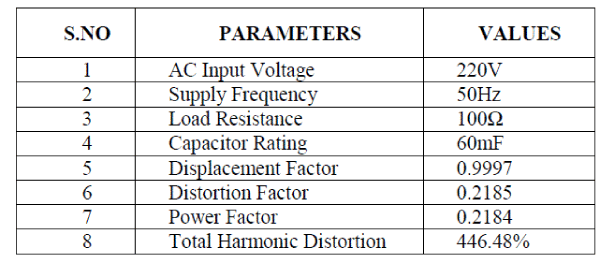 |
| Table II. Results and Values of parameters for AC/DC Single Phase Converter with Capacitive Filter |
 |
| Figure 5: Input Voltage (V), Input Current (A) (scaled up) waveform for Capacitive Filter |
 |
| Figure 6: FFT Analysis of Input Current waveform for Capacitive Filter |
LC Filter in the Output side: |
| Capacitor draws Heavy Inrush Current. When an Inductor is included, results in larger conduction angle of current pulse and thus peak of the current reduces. THD obtained is seen to be lesser than the THD obtained from the Capacitive Filter. The Figure 7 shows the simulation of AC/DC Single Phase Converter with LC Filter in the Output Side with L=1mH and C=60mF. Table III shows the simulation results. |
 |
| Figure 7: MATLAB/Simulink Implementation of AC/DC Single Phase Converter with LC Filter in the Output side |
 |
| Table III. Results and Values of parameters for AC/DC Single Phase Converter with LC Filter in the Output side |
 |
| Figure8: Input Voltage (V), Input Current (A) (scaled up) waveform for LC Filter |
 |
| Figure 9: FFT Analysis of Input Current waveform for LC Filter |
Parallel Resonant LC Filter in the Input side: |
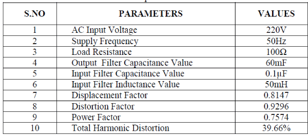
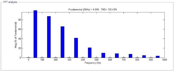
| In the previous two circuits, it is seen that Power Factor is improving and at the same time, THD is also reducing. A Parallel LC Filter tuned to resonate for a Particular Harmonic Frequency is analyzed here. |
 |
| For making the Third Harmonic Impedance infinity (possible only theoretically), we chose 3XL= Xc/3.This value of L and C are used in the simulation shown in the Figure 10. |
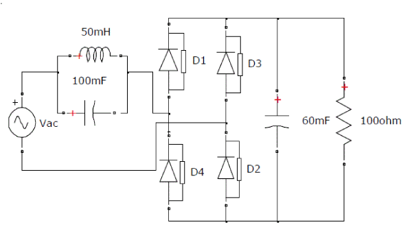 |
| Figure 10: MATLAB/Simulink Implementation of AC/DC Single Phase Converter with Parallel Resonant Filter in the Input side |
 |
| Table IV. Results and Values of parameters for AC/DC Single Phase Converter with Parallel Resonant Filter in the Input side |
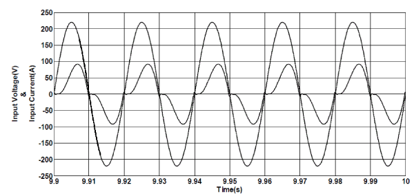 |
| Figure 11: Input Voltage (V), Input Current (A) (scaled up) waveform for Parallel Resonant Filter |
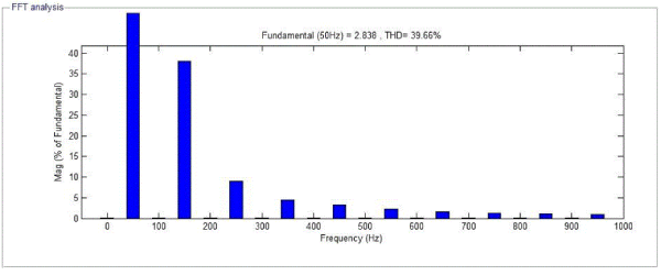 |
| Figure 12: FFT Analysis of Input Current waveform for Parallel Resonant Filter |
Series Resonant LC Filter in the Input side: |
| A Series Resonant Filter is tuned not to allow any Harmonic Frequencies. Further Improvement in Power Factor and Reduction in THD can be seen with Series Resonant Filter. The Values are chosen to satisfy the resonance Condition |
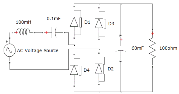 |
| Figure 13: MATLAB/Simulink Implementation of AC/DC Single Phase Converter with Series Resonant Filter in the Input side |
 |
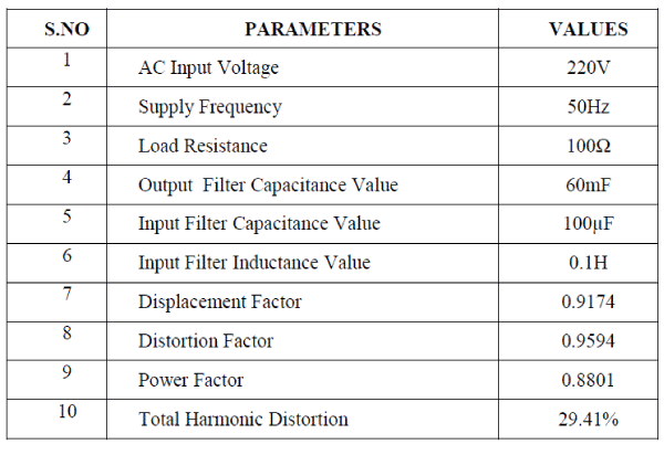 |
| Table V. Results and Values of parameters for AC/DC Single Phase Converter with Series Resonant Filter in the Input side |
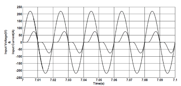 |
| Figure 14: Input Voltage (V), Input Current (A) (scaled up) waveform for Series Resonant Filter |
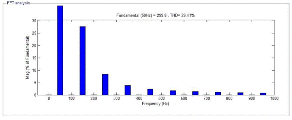 |
| Figure 15: FFT Analysis of Input Current waveform for Series Resonant Filter |
Closed loop Boost Converter in the Output side: |
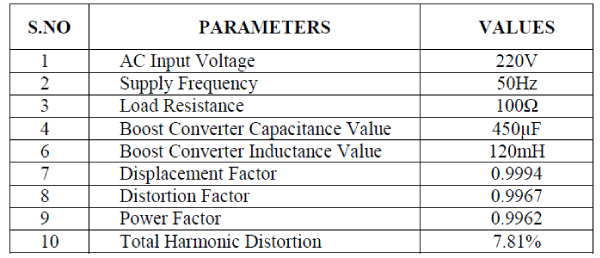
| Boost Converter dynamically regulates the DC bus voltage. The Current through the Inductor is controlled using PWM switched MOSFET in the Boost Converter. The error in DC bus Voltage is multiplied with the unregulated input DC Voltage to the Boost Converter giving the Current reference for the Inductor. This Reference current is used to regulate the Current through the Inductor thereby regulating the DC bus Voltage. The Values of Inductor and Capacitor are chosen as 120mH and 450μF. The Results obtained prove that closed loop control provides near unity Power Factor and the lowest THD level than any of the above discussed circuits. Figure 16 shows the simulation. |
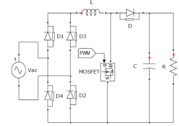 |
| Figure 16: MATLAB/Simulink Implementation of AC/DC Single Phase Converter with Closed loop Boost Converter in the Output side |
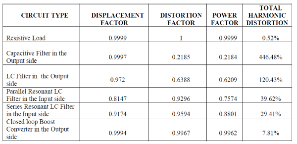 |
| Table VII shows that for a Resistive Load there is almost No Distortion in the Input Current (0.52%). But to eliminate the Output Voltage ripple a capacitor is added. The Addition of a Capacitive Filter at the Output Drastically increases the Distortion in the Input Current. Other Passive filters though increase the Power Factor at the Input and reduce the Distortion, it is seen that only Closed Loop Boost Converter provides Highest Input Power Factor and minimum Total Harmonic Distortion. Closed Loop Regulatory control is the most efficient Power Factor Improvement Method. |
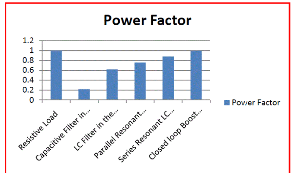 |
| Figure 19: Improvement in Power Factor in the Order of analysis of the circuits |
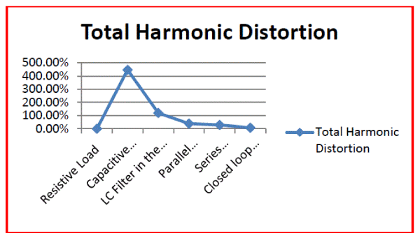 |
| Figure 20: Reduction in THD in the Order of analysis of the circuits |
| Figure 19 and Figure 20 shows the Variation of Input Power Factor and Total Harmonic Distortion of Input Current. The THD results were obtained from FFT Analysis in MATLAB/Simulink. It is observed that for Closed Loop Boost Converter Method the Power Factor is unity. |
HARDWARE IMPLEMENTATION |
| The Closed Loop Boost Converter type circuit is implemented in hardware (Figure 21) using PFC IC. Unregulated DC voltage output and Regulated DC voltage output is shown in Figure 22 (a) and (b). The Ripple is found to be very minimum for Boost Converter Regulated DC Voltage. The Experimental Setup is shown in Figure. The Switching pulse to the MOSFET is generated using PFC IC. (Figure 23) |
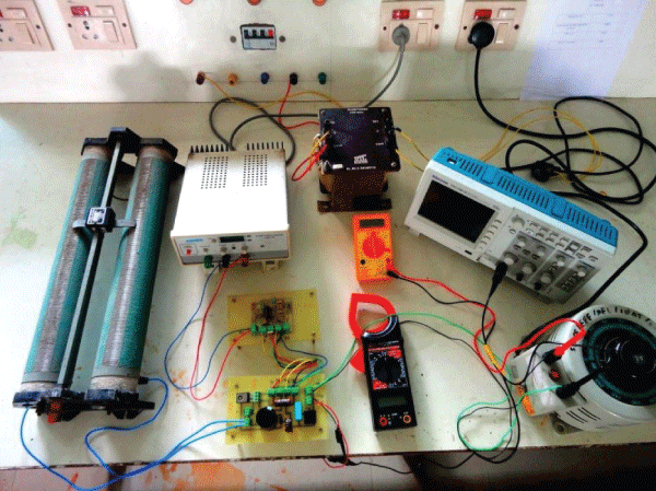 |
| Figure 21: Hardware setup for Closed Loop Boost Converter Controlled AC/DC Single Phase Converter |
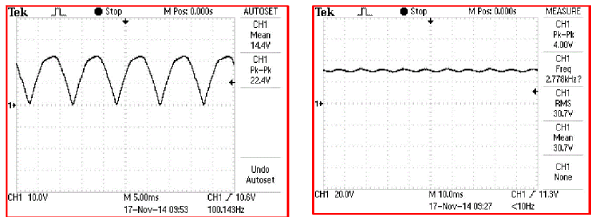 |
| Figure 22: (a) Unregulated DC Output Voltage (b) Regulated DC Output Voltage |
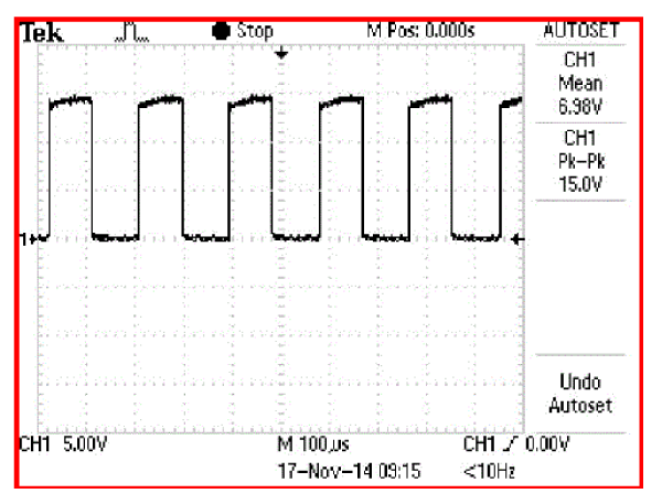 |
| Figure 23: MOSFET Gate Pulse from PFC IC |
CONCLUSION |
| The Investigation of the above circuits showed how Power Factor and THD various by just mere interchanging of the passive elements in the front end and at the back. The Filters need to be carefully tuned. THD can be reduced to only a certain minimum level by using Single Stage filters. The Closed loop regulatory control provides further reduction in THD percentage. By using Boost Converter type regulatory control the THD obtained was approximately 7%. This can be improved to a better level by implementing Interleaved Boost Converter type Control as it provides reduction in Input Current Ripple than to Conventional Boost Converter. |
References |
|