Keywords
|
| buck converter, zero current transition (ZCT), interleaving technique, Switching loss, Conduction loss |
I. INTRODUCTION
|
| Power conversion is in and of itself a general topic, one that is addressed within the fieldof Power Electronics. There are four general forms of power converting circuits ac-to ac,ac-to-dc, dc-to ac, and dc to dc. Power conversion in general is used to provide the correctform of energy needed by the load. Buck converters are step-down DC-DC convertersthat are widely being used in different electronic devices like laptops, cell phones and alsoelectric vehicles to obtain different level of voltages. These converters are nothing but,high frequency switching devices operating on PWM principle. |
| Even though buck converter is commonly used for step down conversion, it has many disadvantages such that low efficiency, high output voltage ripple, unable to operate at high switching frequencies etc. So we are using interleaving technique in buck converters. Interleaving technique can be thought of as a method of paralleling converters. However, it has additional benefits to offer in addition to those obtained from conventional approaches of paralleling converters. Interleaving technique is widely used in personal computer industry to power central processing units [1], [4]. |
| The switching technique used in buck converters for IGBT switching are hard switching and soft switching.Hard Switching occurs when there is an overlap between voltage and currentwhen switching the IGBT on and off. This overlap causes energy loss which can be minimized by increasing the di/dt and dv/dt. However, fast changing di/dt or dv/dt causes EMI to be generated. Therefore the di/dt and dv/dt should be optimized to avoid EMIissues. There are a few additional problems in hard switching. The device stress increases because the switching locus moves through the active region of the safe operating area (SOA).The reliability of the device can be impaired due to prolonged hard switching operation.High dv/dt, di/dt and parasitic ringing effect at switching of a fast device can create severeelectromagnetic interference (EMI) problems, which may affect the converter control circuitand nearby sensitive apparatus [3], [6]. |
| The main idea of soft switching is to prevent orminimize the overlap between the voltage and current so that the switching loss is minimal.Zero current switching (ZCS) and zero voltage switching (ZVS) are two techniques used for soft switching. In the proposed interleaved zero current transition converter soft switching (ZCT) is used, which has some advantages over traditional hard switching.With substantially reduced switching loss, the switching frequency can be increased above the audio frequency range as desired [2]. |
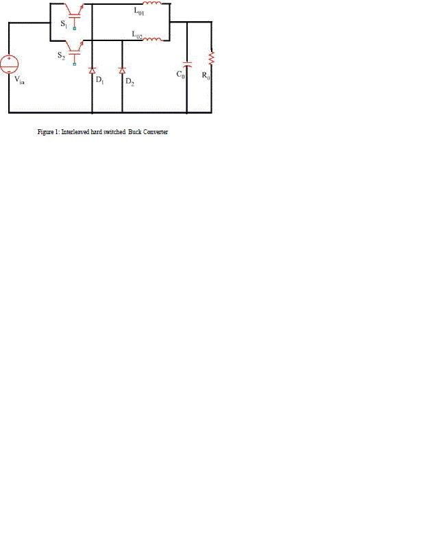
| Interleaved hard switched buck converter is the traditional interleaving technique used for buck converter. Fig.1 shows the traditional interleaved hard switched buck converter. The disadvantage of this converter is that the switching losses are high since hard switching is employed in this configuration. The switching loss in IGBTs and the diode reverse recovery losses are high in this circuit. |
II. INTERLEAVED ZCT BUCK CONVERTER
|
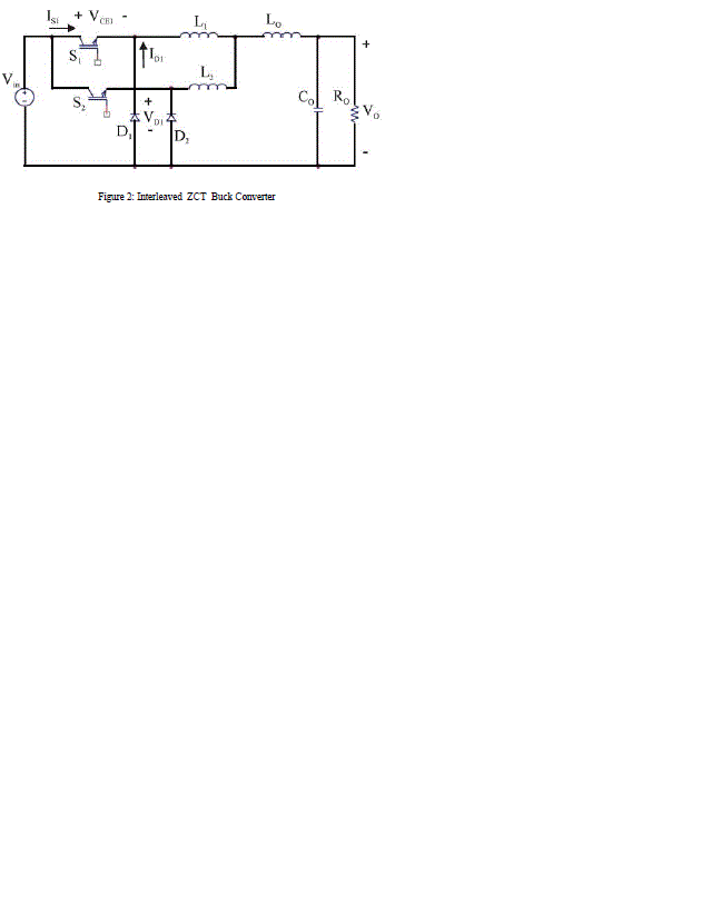
| Interleaved zero current transition (ZCT) buck converter is derived from the standard buck converter. The key modifications include the addition of two small inductors L1 and L2 and the phase shifted operation of the two stages. The phase shifted interleaved operation is thesame as the operation of switches in multiphase converters commonly applied in microprocessor power supplies and inthe interleaved boost PFC rectifiers. Fig.2. shows interleavedZCT buck converter. |
| Compared with the standard hard-switched PWM converter, each switch in interleavedZCT buck converter operates at two times lower switching frequency and conducts half ofthe time. Furthermore, both switches in the interleaved ZCT configuration participate inthe power processing function of the converter and share the power equally. The small auxiliary inductors L1 and L2 enable the ZCT turn-on and reduced switching losses, whereasthe larger inductor L0 results in a continuous conduction mode (CCM) of operation withgood average current sharing and low current ripple, which is well suited for plasma power supplies. |
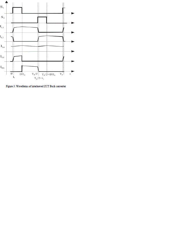
| The circuit operations in one switching cycle can be divided into six stages. The key waveforms of these stages are given in Fig. 3. |
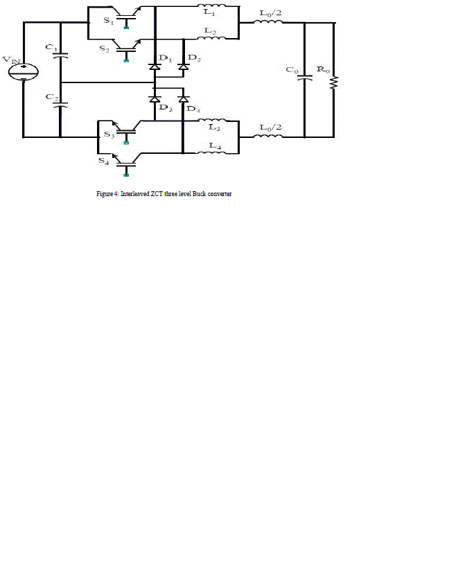
| Interleaved zero current transition buck converters can be modified to an Interleavedzero current transition three level buck converter. Fig.3.2 shows an Interleaved zero currenttransition three level buck converter. |
III. SIMULATION RESULTS
|
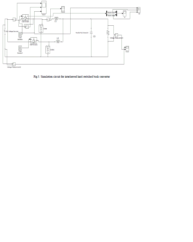
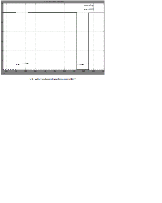
| The simulations of different circuits are done with the help of MATLAB. The circuit used forsimulation of interleaved hard switched buck converter is shown in fig.5.There are twoIGBTs used in the circuit. The two IGBTs are switched at 16 kHz frequency and thus theeffective switching frequency is 32 kHz.Fig.6 gives the current and voltage waveforms across the IGBT. An overlapping between current and voltage waveforms occurs because of the switching losses. |
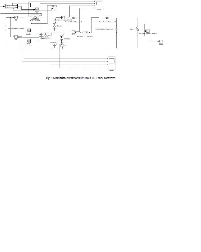
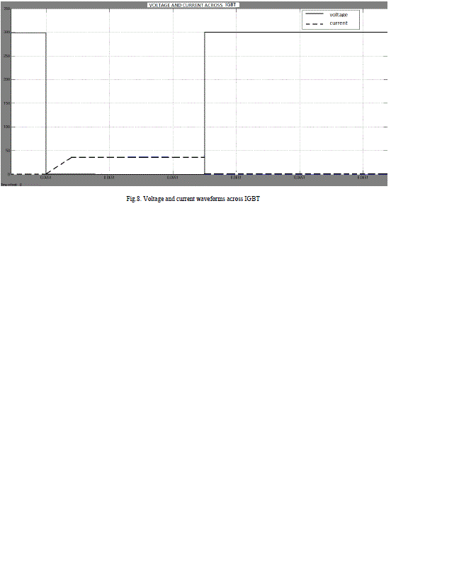
| The circuit used forsimulation of interleaved ZCT buck converter is shown in fig.7.There are twoIGBTs used in the circuit. The two IGBTs are switched at 16 kHz frequency and thus theeffective switching frequency is 32 kHz.Fig.8 gives the current and voltage waveforms across the IGBT. Current increases just after the voltage become zero. Thus a zero current turn on is obtained. This helps in reducing switching losses. |
IV. LOSS CALCULATION USING PSIM
|
| The IGBT switching losses and conduction loss are calculated using Powersim(PSIM).PSIMis the leading simulation and design software for power electronics, motor drives, and dynamic system simulation. With fast simulation and easy-to-use interface, PSIM provides apowerful and efficient environment to meet our simulation needs.In order to calculate the loss we need Thermal module. Thermal Module is an add on option to the PSIM software. It allows users to add semiconductor device data sheetinformation into a database, and use these devices in the simulation for the loss calculation.Thermal Module provides a quick way of estimating device conduction losses andswitching losses [7]. |
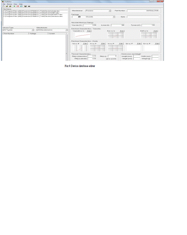
| In this example an IGBT Powerex CM150du-24nfh is added to the database. So we will create a new device file called Powerex.dev, and we will place it in the 'device' sub-folder inPSIM. Go to File > New Device File, and under the PSIM device sub-folder, create the file Powerex.dev. This file will appear in the File Name list box at the upper left corner ofthe Device Database Editor to create the thermal module. Device database editor is shown in fig.9. We have to add different electrical characteristics of IGBT to device data editor. Once the thermal moduleis created it can be used for loss calculation. |
| Fig.10. shows the thermal module of an IGBT. There are 4 extra nodes on each thermalmodule of IGBT than the normal IGBT. These 4 nodes are for the power losses, and theyare (from top to bottom): transistor conduction losses , transistor switching losses, diode conduction losses and diode switching losses. They are inthe form of electric currents, and will flow out of these nodes. To measure the losses values,connect an ammeter to each node. |
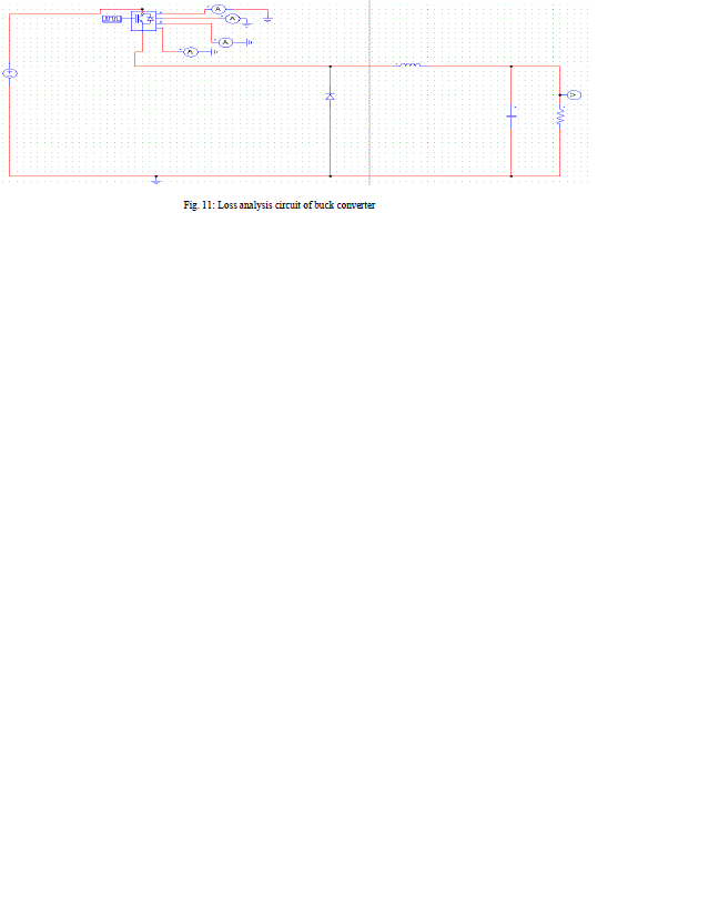
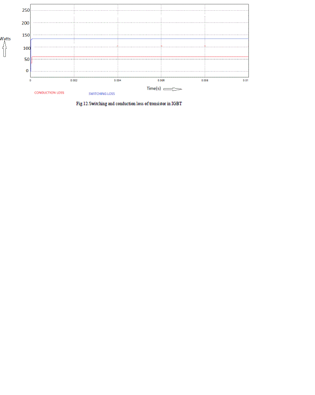
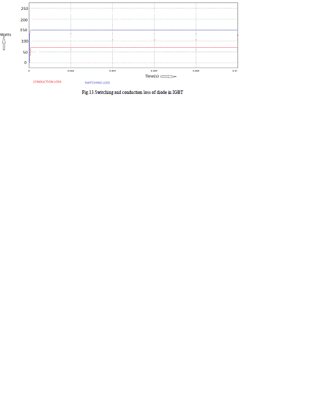
| Fig.11, Fig.12 and Fig.13 shows the loss calculation circuit of standard buck converterand the switching loss and conduction loss of transistor andswitching loss and conduction loss ofdiode in IGBTs of the buckconverter.The switching frequency used is 32 kHz. The input voltage is 300v. |
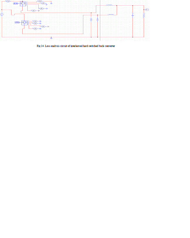
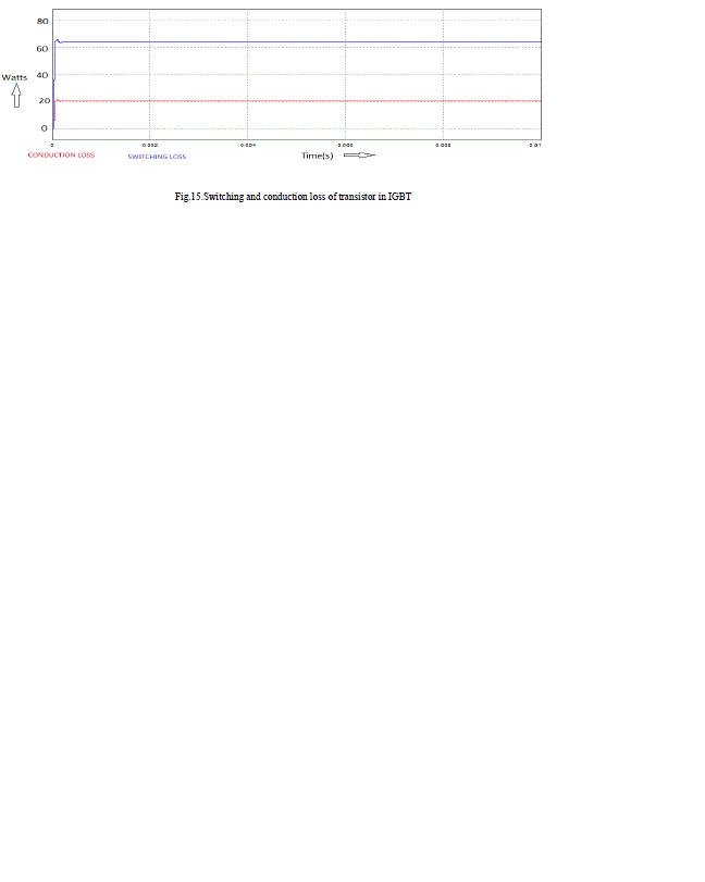
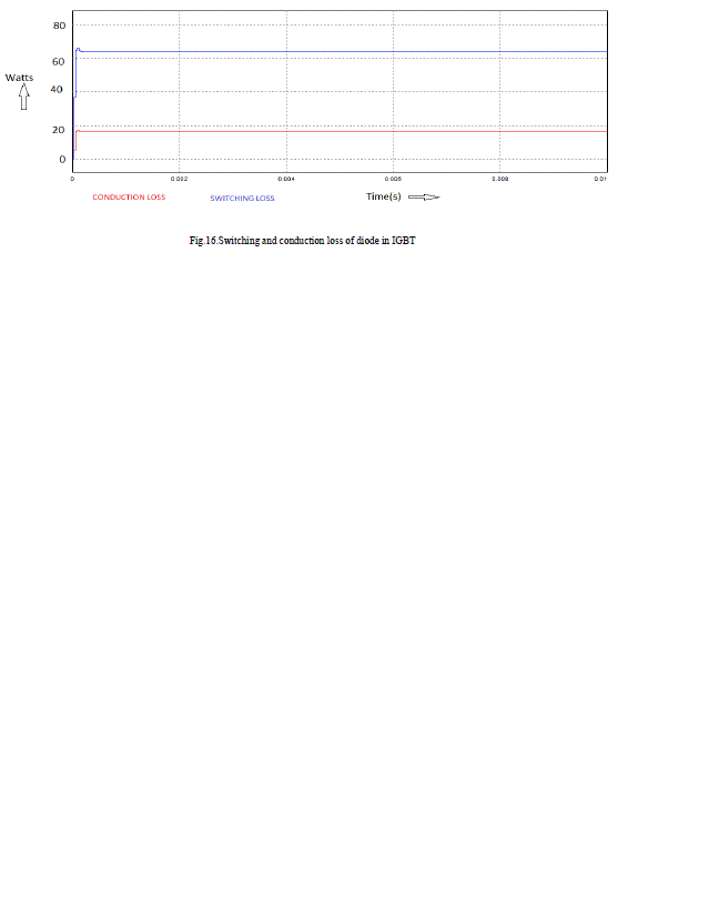
| Fig.14,Fig.15 and Fig.16 shows the loss calculation circuit of interleaved hard switched buck converterand the switching loss and conduction loss of transistor andswitching loss and conduction loss ofdiode in IGBTs of theconverter. The switching frequency used is 16 kHz for each IGBT. Thus the effective switching frequency is 32 kHz. The input voltage is 300v. |
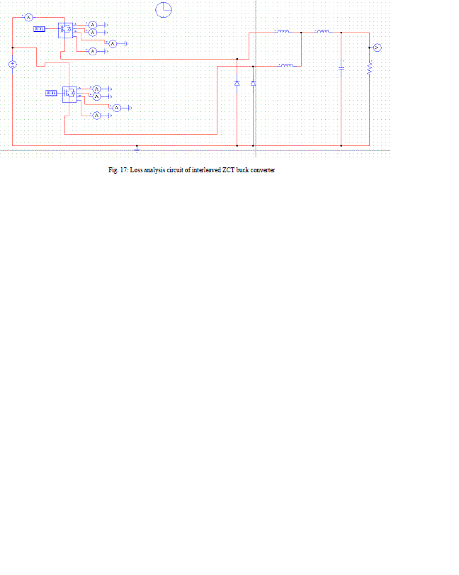
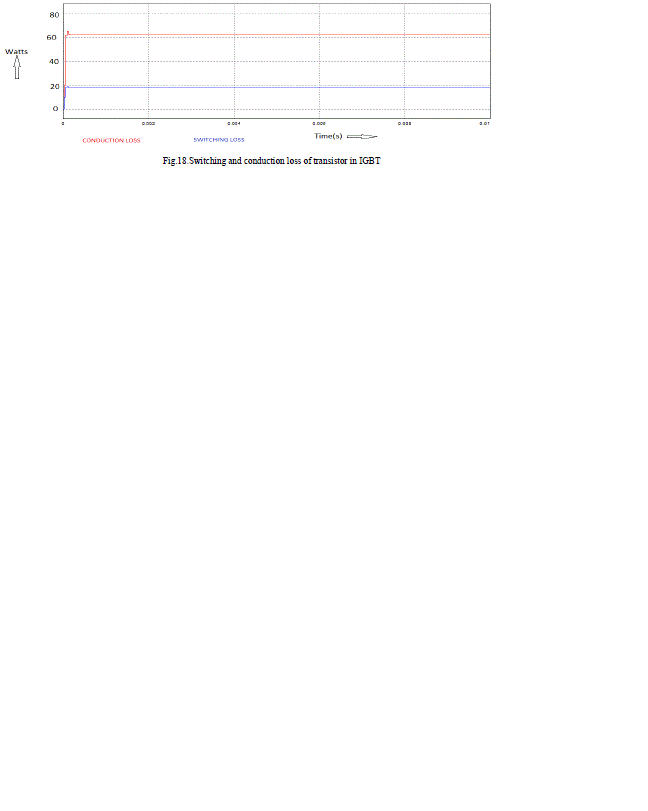
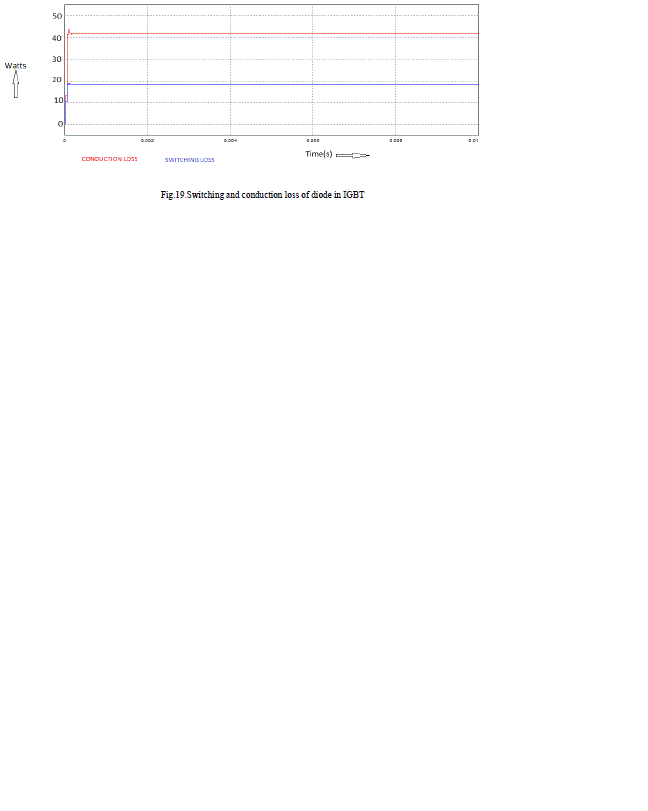
| Fig.17,Fig.18 and Fig.19 shows the loss calculation circuit of interleaved ZCT buck converterand the switching loss and conduction loss of transistor andswitching loss and conduction loss ofdiode in IGBTs of the converter. The switching frequency used is 16 kHz for each IGBT. Thus the effective switching frequency is 32 kHz. The input voltage is 300v. |
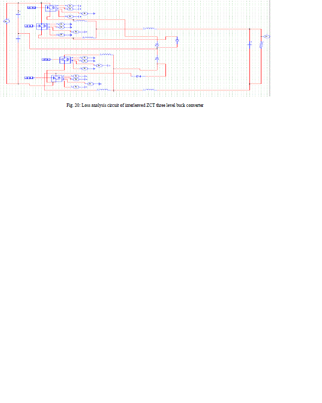
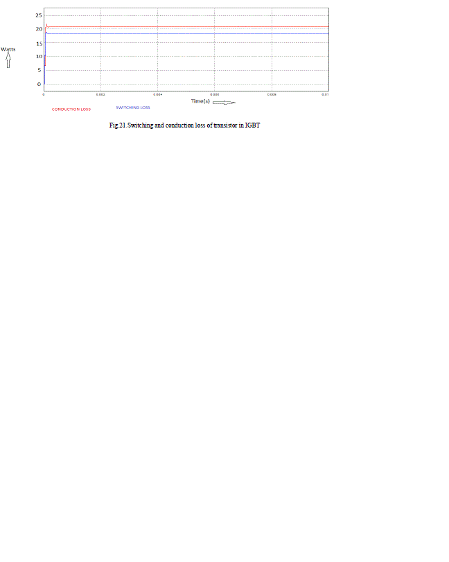
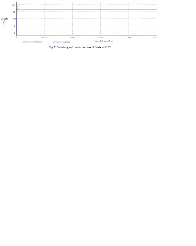
| Fig.20,Fig.21 and Fig.22 shows the loss calculation circuit of interleaved ZCTthree level buck converterand the switching loss and conduction loss of transistor andswitching loss and conduction loss ofdiode in IGBTs of the converter. The switching frequency used is 8 kHz for each IGBT. Thus the effective switching frequency is 32 kHz. The input voltage is 300v. |
| From the graph of switching loss and conduction loss of hard switched interleaving buck converter and interleaved zero current transition buck converters it is clear that the switching loss and conduction loss of hard switched interleaving buck converter is higher than that of interleaved zero current transition buck converters.The switching losses of buck converter,interleaved hard switched buck converter,interleaved ZCT buck converter andinterleaved ZCT three level buck converters are tabulated below. |
V. EXPERIMENTAL RESULTS
|
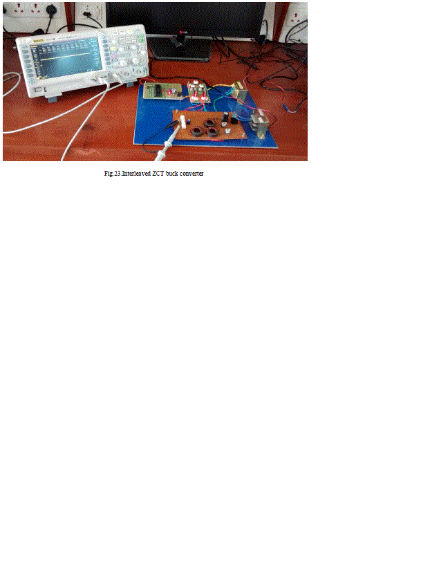
| The experimental setup of proposed interleaved ZCT buck converter is shown in figure 23. In experiment a 230/12V transformer with rectifier is used for DC input. In order toturn on the switch, switching pulses are required and it is developed using PIC 16F877Amicro controller.The pulses obtained from the micro controller are around 5V, which is notenough to turn on the switch. Hence a driver circuit is used to boost the voltage triggeringsignal to 9V to 20V.The driver circuit forms the most important part of the hardware unit,because it gives the triggering pulse to the switches in the proper sequence. |
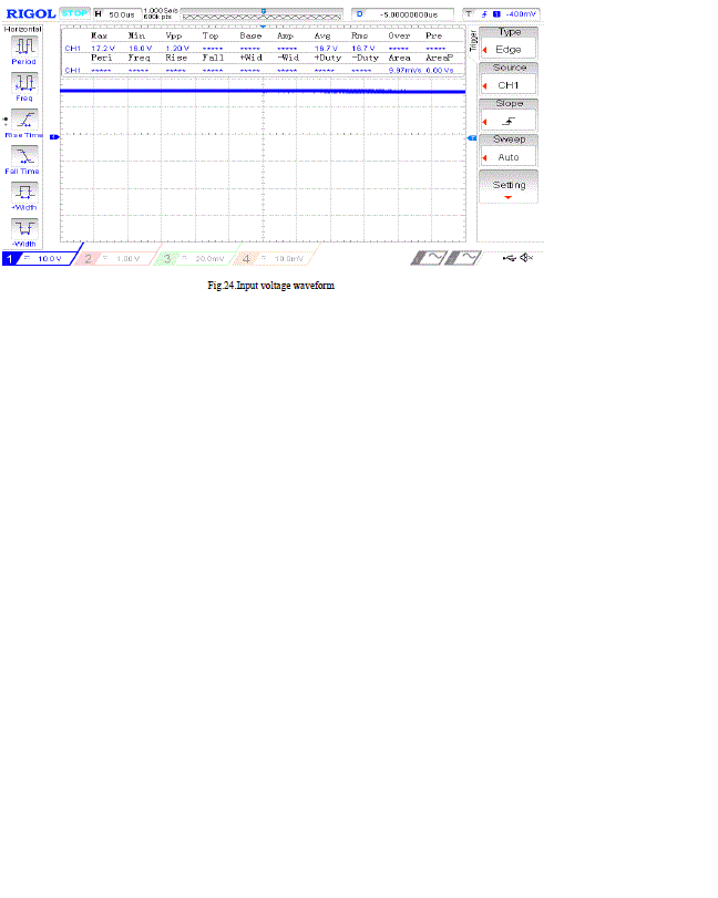
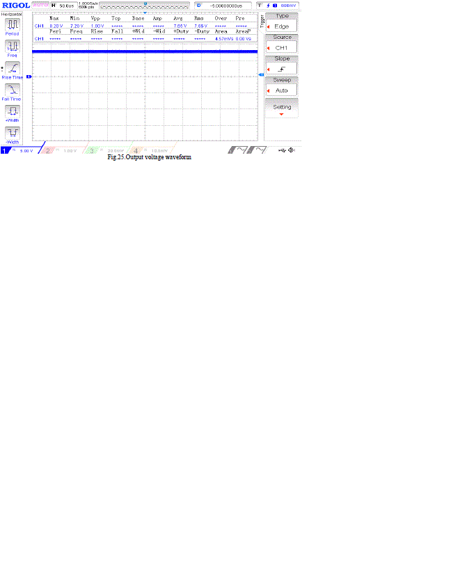
| For the proposed model, it is provided with a 16 V DC supply and obtained a 7.2 V output. Theswitching frequency is 16 kHz. The switching pulses are developed using PIC 16F877A micro controller. Figure 24 shows the input voltage waveform. Figure 25 shows outputvoltage waveform. |
VI. CONCLUSION
|
| The concept of zero current transition isintroduced in interleaved buck converters. In the proposed interleaved ZCT converters the switches are operating out-of-phase.The turn-on transitions at zero current and a significant reduction of the losses associated with the diode reverse recovery are accomplished through the addition of two small inductors.The output voltageripple is also minimized in the proposed interleaved ZCT buck converter.Also the loss inIGBT is calculated using thermal modules in PSIM.From the thermal module calculationof switching losses, proposed interleaved zero current transition converter has minimum losscompared with the interleaved hard switched buck converter. |
| |
Tables at a glance
|
 |
| Table 1 |
|
| |
Figures at a glance
|
 |
 |
 |
 |
 |
| Figure 1 |
Figure 2 |
Figure 3 |
Figure 4 |
Figure 5 |
|
 |
 |
 |
 |
 |
| Figure 6 |
Figure 7 |
Figure 8 |
Figure 9 |
Figure 10 |
|
 |
 |
 |
 |
 |
| Figure 11 |
Figure 12 |
Figure 13 |
Figure 14 |
Figure 15 |
|
 |
 |
 |
 |
 |
| Figure 16 |
Figure 17 |
Figure 18 |
Figure 19 |
Figure 20 |
|
 |
 |
 |
 |
 |
| Figure 21 |
Figure 22 |
Figure 23 |
Figure 24 |
Figure 25 |
|
|
| |
References
|
- Milan Ilic and DraganMaksimovic, "Interleaved zero current transition buck converter," IEEE Transactions on industry applications, vol. 43, no.6, Nov/Dec 2007.
- G.Hua,E.Yang and Y.Jiang, "Novel zero current transition PWM converters ," inProc.IEEE PESC,1993.
- Bose, B.K, "Need a Switch," IEEE Industrial Electronics Magazine, Volume 1 issue 42007.
- Milan Ilic and DraganMaksimovic, "Interleaved zero current transition three-levelbuck converter," in Proc.IEEEAPEC ,2006.
- Powerex cm150du-24nfh data sheet.Available: http://www.pwrx.com/pwrx/docs/cm150du-24nfh.pdf
- F. Canabals, P.barbosa and F.C. Lee,"A zero-voltage and zero-current switching threelevel buck converter",IEEE Transactions on powerelectronics, vol.17, Issue 6, Nov2002.
- "IGBT loss calculation using the thermal module", Available atwww.powersimtech.com.
|