ISSN ONLINE(2319-8753)PRINT(2347-6710)
ISSN ONLINE(2319-8753)PRINT(2347-6710)
Shiv Kumar Choubey1, K.P.Tiwary2*
|
| Related article at Pubmed, Scholar Google |
Visit for more related articles at International Journal of Innovative Research in Science, Engineering and Technology
The nanoparticles of CdS were successfully synthesized by Microwave assisted irradiation method. CdS materials can be used for the fabrication of solar cells, nonlinear optical materials, optoelectronic and electronic devices. X-ray diffraction (XRD) and scanning electron microscopy (SEM) technique were used for structural and morphological characterization of nanoparticles of CdS. XRD characterization of nanoparticles were taken which verify the crystalline form. The average size of the nanocrystallites were measured by Debye-Scherrer formula as per the XRD spectrum and the particle size lies in the range 4 - 7 nm. The optical characterization of the nanoparticles of CdS were taken by UV-Visible absorption spectra and the optical bandgap of as synthesized CdS nanoparticles were found to be 3.8 eV.
Keywords |
| Microwave, XRD, bandgap, nanoparticles |
INTRODUCTION |
| II-VI compound semiconductors such as ZnS, CdS, CdSe, etc., are promising materials for technological application, mostly due to their large band gap. In recent years there has been increased interest in the scientific and technological aspects of the nanosized semiconductors. Semiconductor nanocrystals have received much attention recently due to their size dependent optical properties and and their applications as light emitting diode, phosphors in lighting, displays, solar cell, X-ray sensors, photocatalyst and electrochemical cell [1-5]. Semiconductor nanomaterials are of great interests for both fundamental research and industrial development. II-VI semiconductor nanocrystals have been synthesized by a variety of methods which include solvothermal method, co-precipitation method, sol-gel process, chemical bath deposition method and microwave irradiation method [6-9]. The formation of high quality nanocrystals can be achieved by controlling the thermodynamics and kinetics during the nucleation and its growth [10]. |
| Water has a very high dipole moment and that is why it is one of the best solvent for microwave assisted reaction [11]. During the formation of the nanoparticles under microwave irradiation, solvents can have an important influence on the size and morphology of the final products. Among II-VI semiconductors, CdS is a widely used substance with many advanced technological application. It is one of the most studied materials with a direct band gap of 2.42 eV. By controlling the size of the nanoparticles, it is possible to design a material of required magnetic, elastic and optical properties. In different solvents, the collision rate between reactant molecules, the heating rate, and the temperature of the reaction are different [12]. Microwave heating results from the interaction of the electromagnetic wave with the irradiated medium which produce a force on charged particles and cause them to rotate or further polarized. In this paper we report the synthesis of CdS nanoparticles by microwave assisted methods and their optical characterization. |
II. EXPERIMENTAL |
Synthesis: |
| CdS nanoparticles were synthesized by microwave assisted technique. All the chemicals used in the synthesis were taken of AR grade and were used without further purification. For the synthesis of CdS nanoparticles, aquous solution of Cadmium acetate (Cd(CH3COOH)2.2H2O) and thioacetamide (CH3CSNH2) were prepared and stoichiometrically combined. Molar concentration of (Cd(CH3COOH)2.2H2O) was taken as 0.5 M and the molar concentration of thioacetamide was taken relatively a little more. The solution was further diluted with distilled water and the volume of the solution was made to 400 ml and it was kept on magnetic stirrer for an hour to make the solution homogeneous. The solution was then microwaved (LG make microwave oven) with a power of 900W for a period of 6 minutes and a duty cycle of 25%. Microwave irradiation time was 20 sec (t1), Rest period was 60 sec (t2) then duty cycle |
 |
| The reaction was completed in 6th cycle and Cadmium sulphide got precipitated. As the precipitation formation get started, the solution was removed from microwave, washed with distilled water and dried at 700C for 6 hours in an oven. |
Characterization: |
| When the nanoparticles of Cadmium sulphide as synthesized were well dried then it was characterized for structural and optical properties. The X-ray diffraction patterns of the samples were recorded by Rigaku X-ray diffractometer with a CuK radiation ( ) in a range of from 200 to 700. The Scanning Electron Microscope technique is a common way to observe the morphology of the samples. SEM Micrograph of the nanoparticles of CdS was taken to observe the surface morphology. For optical characterization the absorption and transmittance spectrum were recorded using UV-Vis spectrometer (Rayleigh UV-2601). The optical absorption spectrum was carried out in the wavelength range of 200 – 1200 nm. The energy band gap of the prepared material was also calculated by taking optical absorption spectrum. |
III. RESULT AND DISCUSSION |
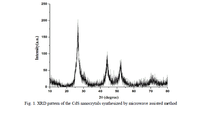
| The as prepared CdS nanoparticles were characterized by X-ray diffractometer. Fig. 1 shows the X-ray diffraction pattern of CdS nanocrystals synthesized by microwave assisted technique. |
 |
| The X-ray diffraction of the samples were recorded by an X-ray diffractometer with a Cu radiation ( ) in a range of from 100 to 800. The major peaks are identified at 2θ equal to 26.60, 44.30 and 52.00 which corresponds to the crystal planes (111), (220) and (311) respectively in cubic phase. The diffraction peaks in the pattern can be indexed well to the cubic structure of CdS (JCPDS 10 - 454). |
 |
| Using Debye- Scherrer formula [13], the crystallite size of the synthesized CdS was calculated from full width at half maxima of Xrd pattern shown in Fig.1. The average nanocrystallite size is calculated by the formula, |
 |
| Where is the Bragg’s angle, is the wavelength of the incident ray and is the full width at half maxima. The average size of the nanoparticles was calculated to be 6 nm. The broadening of the diffraction peak in the xrd pattern may ensures the formation of the nanocrystallinity. |
 |
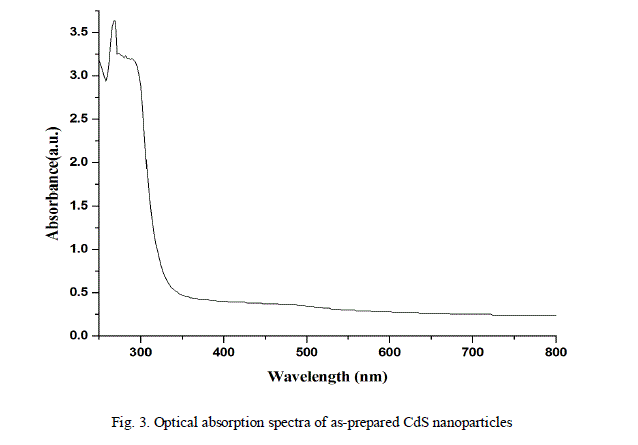
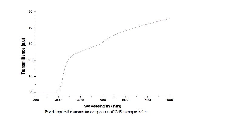
| The optical absorption and transmittance of the semiconductor nanoparticles are one of the important properties to be studied to understand the behaviour of the nanoparticles. The absorption and transmittance spectrum of CdS nanoparticles were taken in the wavelength range 250 - 800 nm which is shown in Fig.3. and Fig.4. The characteristic absorption peaks are appeared in the wavelength range 300 - 400 nm and the peak position reflects the band gap of the nanoparticles. |
 |
| The energy band gap of the CdS nanoparticles was evaluated by Tauc relation [14], plotting a graph between versus and by extrapolating the linear region of the curve to the energy axis. |
| Where α is the absorption coefficient, hv is the photon energy, Eg is the direct band gap energy, and is a constant. Fig. 5 shows the graph between versus , where the intercept of the graph on X- axis gives the value of band gap which is equal to 3.81 eV. |
IV. CONCLUSION |
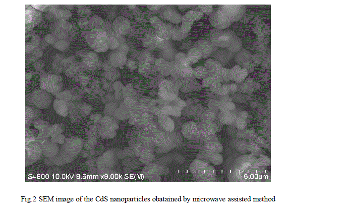
| The nanoparticles of CdS were successfully synthesized by microwave assisted technique using Cadmium acetate (Cd(CH3COOH)2.2H2O) and thioacetamide (CH3CSNH2) in aquous medium. The crystal structure and the crystallite size of the particles were obtained using X-ray diffractometer. CdS nanoparticles of cubic phase with an average crystallite size of around 6 nm were obtained. SEM micrograph shows the formation of spherical CdS nanoparticles.. The optical band gap of the nanoparticles of CdS were obtained from UV-Vis absorption spectrum which was calculated to be 3.81 eV. It has been observed that the reaction rate is faster in case of microwave assisted synthesis. It was also concluded that the optical band gap of the microwave assisted synthesized CdS was found to be increased as compared to that of the bulk CdS. |
References |
|