Keywords
|
| Optoelectronic, Photoswitche, Coplanar line, MSM-Photodetector, Semiconductor. |
INTRODUCTION
|
| A photoswitch is a component that can change its impedance from a very low value to a high value in a short time with a high accuracy and repeatability. The first photoswitch was made in 1975 by D.H. Auston [1], the latter was constituted of an interrupted microstrip line. The whole was performed on a high resistive silicon substrate, and continuously supplied with a DC voltage. To improve the switching from one state to the other, R. Castagné et al have introduced the use of coplanar waveguide lines technology instead of microstrip line [2]. The major shortcoming of these first photoswitches was the repetition frequency, due to the carriers’ life time in the silicon. To overcome this disadvantage, the concluded action was to use substrates having a shorter carriers’ life time such as GaAs [3] or InP [4]. Researches aiming at the realization of the microwave circuits and the optical command on a single substrate was made as well [5-7]. Other researchers have focused on the use of a photoswitch based on low temperature GaAs (LT-GaAs) [8-9] and more recently [10-14] for the sampling function and the fast sampling, respectively. |
| This paper is divided into five parts, the second part explains the operating principle of photoswitch. The third one is devoted to the characterization of photoswitches introducing single-electrode MSM photodetectors with linear tapers. The photoswitches performance optimization by the introduction of new topologies of coplanar lines with sinusoidal and exponential shaped tapers, then by the tightening of ground planes around the central strip are presented in the fourth section. Finally, a conclusion is drawn to make a summary of the obtained results and to quote some possible prospects of this work. |
II.FUNCTIONING OF PHOTOSWITCH
|
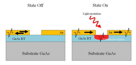
| The device operates as an optically controlled switch. In its simplest form, the photoswith is represented by an interrupted microwave line. When this interruption is illuminated by an optical beam whose photon energy is greater than the band gap energy of the semiconductor on which the coplanar line is lay (LT-GaAs absorbent at 0,8 μm in our case), the latter becomes conductive by photoconduction (state On). In contrast, in darkness, the signal is reflected (state Off), the photoswitch’s principle is illustrated in figure 1. |
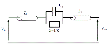
| The interruption can be modeled as a first approximation by a photoresistor in parallel with a capacity (Auston’s model [1]) figure 2. Then, in darkness, photoswitch behaves essentially as a capacitor, the microwave insulation is as stronger as the signal frequency is low. Under illumination, the photoswitch behaves as a resistor, the signal level does not depend on its frequency. The aim is to increase the insulation at the Off state and reduce the insertion losses at the On state. |
III.CHARACTERIZATION IN DARKNESS OF THE SINGLE-ELECTRODE PHOTOSWITCH WITH LINEAR TAPERS
|
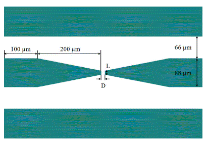
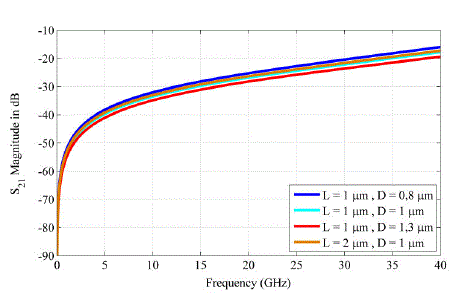
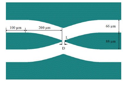
| The characterization of single-electrode photoswitch in darkness which we have made, concerns the measuring of the reflection and transmission coefficients of the microwave signal, S11 and S21 respectively, on a frequency range of 0-40 GHz. In order to achieve submicron line widths, it is necessary to use tapers for gradually adapt the electromagnetic wave, limiting losses as well. The measurements were carried out on the coplanar lines introducing single-electrode MSM photodetectors (figure 3) with parameter D value (interruption distance) equal to 0.8, 1 and 1.3 μm and parameter L value (interruption width) equal to 1 and 2 μm. Remembering that the access contacts have been designed in such a way that give a characteristic impedance of 50 Ohms, with a central strip’s width of 88 μm, and with a distance between the central strip and the ground plane of 66 μm by taking as reference frequency 20 GHz. |
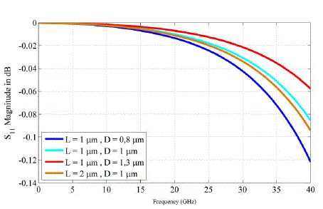
| Figures 4 and 5 show the evolution in darkness of the reflection (S11) and the transmission (S21) coefficients, these results indicate that the parameters L and D have very small influence on the reflection coefficient as well as the insulation when the microwave lines are measured in darkness. The insulation varies between -25 and -28 dB at 20 GHz whatever the value the D and L parameters, which seems logical, since the wavelengths at these frequencies are just few millimeters, about three or four times the interruption’s dimensions. In this case, only the interruption capacity is involved in the stoppage of the microwave signal. This first study validates the fact that a submicron interruption can almost stop the signal propagation. However, with an insulation of -28 dB, it is necessary to optimize these lines in order to reduce the existing coupling between both ends of the interruption to reach a good value the On/Off ratio of the photoswitch (>40 dB). |
IV.OPTIMIZATION OF PHOTOSWITCH
|
A. Optimization by introducing tapers of sinusoidal and exponential shapes
|
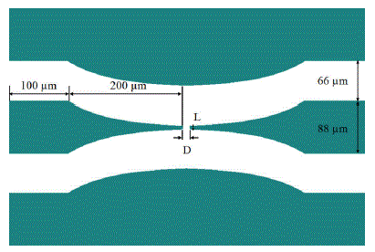
| The optimization goal is to increase the insulation in darkness, to do so, new topologies of coplanar lines introducing tapers of sinusoidal and exponential shapes are proposed. The tapers’ role is to allow the electromagnetic field to gradually adapt and to reduce the impedance’s variations. Figures 6 and 7 represent the topologies of photoswitches having a sinusoidal and exponential tapers’ configuration, respectively. With the interruption of dimension L and D. It is worth noting that the distance between the central strip and the ground planes in both cases, is kept constant. |
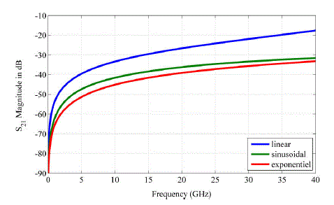
| Figures 8 shows the evolution of the transmission coefficient (S21) in darkness, for the different forms of tapers (linear, sinusoidal, exponential) in the case of an interruption distance D = 1 μm and an interruption width L = 1 μm. We notice that the obtained insulation with the sinusoidal topology is in the range of -36 dB at 20 GHz, while it is of the order of - 39 dB for the exponential configuration at the same frequency value. These results show a good improvement compared to origin device (linear) that was at -26 dB. This improvement can be explained by the fact that the tapers of the sinusoidal and exponential type allow a much more linear transition of the impedance than the triangular tapers. Note that the S11 (not shown in this paper) of all devices disregarding the frequency value are almost similar, (close to 0 dB). |
B. Optimization through the ground planes tightening around the central strip
|
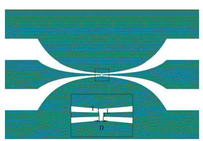
| The topology of the coplanar lines involving a tighter ground planes around central strip is shown in Figure 9 in the case of an exponential configuration of the tapers associated with a tightening distance of T μm. |
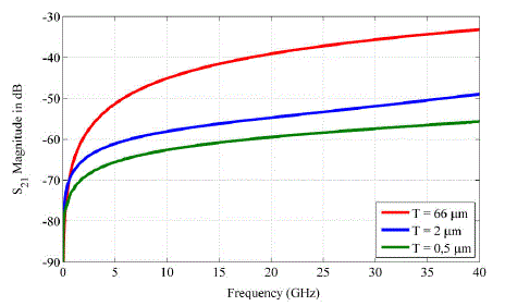
| Figure 10 shows the evolution of the transmission coefficient for a topology with tapers having an exponential configuration and a tightening of mass T of 66, 2 and 0,5 μm, with L and D equal to 1 μm. The obtained results prove the existence of a great improvement in insulation thanks to the tightening of mass. An insulation value at 20 GHz of about -59 dB was achieved in the case of a tightening of 0.5 μm, a gain of about 20 dB compared to the case without tightening. To explain this phenomenon, we can hypothesize that the tightening of the masses leads to a concentration of electromagnetic field and thus the field lines. We can therefore assume that this strong confinement allows the interruption to be much more effective in stopping the microwave signal. |
V. CONCLUSION
|
| In this paper, the characterization of photoswitches consisting of a coplanar line introducing single-electrode MSM photodetectors in the central strip, were presented. The evolution in darkness of the reflection and the transmission coefficients allowed us to explain the influence of various dimensional parameters on the microwave insulation. The performance optimization of photoswitch by introducing new more complex tapers’ shapes: sinusoidal, exponential and by tightening of mass plans around the center strip as well, made it possible to achieve high microwave insulation, of the order of -59 dB, which seems to be quite enough to have a good On/Off ratio of the photoswitch. |
| The prospects of this work are numerous, better results can be achieved if a compromise between the different geometrical parameters could be found. It would also be interesting to realize these components on GaInAs / AlInAs absorbent at 1.55 μm, in order to use compact optical sources developed for telecommunications applications. |
| |
Figures at a glance
|
 |
 |
 |
 |
 |
| Figure 1 |
Figure 2 |
Figure 3 |
Figure 4 |
Figure 5 |
 |
 |
 |
 |
 |
| Figure 6 |
Figure 7 |
Figure 8 |
Figure 9 |
Figure 10 |
|
| |
References
|
- D.H. Auston, “Picosecond optoelectronic switching and gating in silicon”, Applied Physics Letters, vol. 26, no. 3, pp.101-103, 1975.
- R. Castagné, S. Laval and R. Laval, ”Picoseconds-wavelength optoelectronic gate”, Electronics Letters, vol. 12, no. 17, pp.438-439, 1976.
- C.H. Lee, “Picosecond optoelectronic switching in GaAs”, Applied Physics Letters, vol. 30, no.2, pp. 84-86, 1977.
- F.J. Leonberger and P.F. Moulton, “High-speed InP optoelectronic switch”, Applied Physics Letters, vol. 35, no. 9, pp.712-714, 1979.
- U. Hilleringman and K. Goser, “Optoelectronic system integration on silicon: waveguides, photodetectors and VLSI CMOS circuits on onechip”, IEEE Transactions on Electron Devices, vol. 42, no. 5, pp.841-845, 1995.
- P. Freeman, X. Zhang, I. Vurgaftman, J. Singh and P. Bhattacharya, “Optical control of 14GHz MMIC oscillator based on InAlAs/InGaAsHBT’s with monolithically integrated optical waveguides”, IEEE Transactions on Electron Devices, vol. 43, no. 3, pp. 373-378, 1996.
- S. Chouteau, “Intégration de la commande optique d’un commutateur microonde en technologie coplanaire sur silicium”, PhD Thesis,National Polytechnic Institute of Grenoble, 1997.
- N. Zamdmer, Q. Hu, K. A. Mcintosh & S. Verghese, “Increase in response time of low-temperature-grown GaAs photoconductiveswitches at high”, voltage bias. Applied Physics Letters, vol.75, pp.2313-2315, 1999.
- R. Urata, R. Takahashi, V. Sabnis, D. Miller and J.S. Harris, “Ultrafast differential sample and hold using low-temperature-grown GaAs MSMfor photonic A/D conversion”, IEEE Photonics Technology Letters, vol.13, pp.717 -719, 2001.
- C. Tripon-Canseliet, “Commande optique de circuits micro-ondes, Application à la modulation et à l'échantillonnage”, PhD Thesis, Universityof Paris 6, 2003.
- C. Tripon-Canseliet, S. Faci, K. Blary, F. Deshours, G. Alquié, et al. "Optically-controlled microwave phase shifting and sampling by efficientphotoconductive switching on LT-GaAs substrate integrated technology", Proc. SPIE 6343, Photonics North 2006, 63432K, 2006.
- J. Delord, J. Roux, J. Coutaz & N. Breuil “Study of Optoelectronic Sampler Linearity for Analog-to-Digital Conversion of RF Signals”, IEEEPhotonics Technology Letters, vol.21, pp.1369 -1371, 2009.
- J. DELORD, ”Echantillonnage photoconductif de signaux hyperfréquence”, PhD Thesis, University of Savoie, 2010.
- J. Roux, J. Delord and J. Coutaz, “RF Frequency Response of Photoconductive Samplers”, IEEE Journal of Quantum Electronics, vol.47,pp.223 -229, 2011.
|