Keywords
|
| Application-specific integrated circuit (ASIC), area-efficient CSLA, low power |
INTRODUCTION
|
| When we draw a block diagram or circuit diagram we define an input or output. However fast hardware is the gates or other things we have inside the circuit there will be a finite delay in the transmission of a signals this time is defined as propagation delay, of course depends on the length of the signal path as soon as the gates start switches transmission starts. When we want to design the fast circuit or fast system naturally we have to go for some solutions. And also the Design of area- and power-efficient high-speed data path logic systems are one of the most substantial areas of research in VLSI system design. In digital adders, the speed of addition is limited by the time required to propagate a carry through the adder. The sum for each bit position in an elementary adder is generated sequentially only after the previous bit position has been summed and a carry propagated into the next position. |
| The CSLA is used in many computational systems to alleviate the problem of carry propagation delay by independently generating multiple carries and then select a carry to generate the sum . However, the CSLA is not area efficient because it uses multiple pairs of Ripple Carry Adders (RCA) to generate partial sum and carry by considering carry input Cin=1 and Cin=0 then the final sum and carry are selected by the multiplexers (mux). |
| The basic idea of this work is to use Binary to Excess-1 Converter (BEC) instead of RCA with Cin=1 in the regular CSLA to achieve lower area and power consumption [2]–[4]. The main advantage of this BEC logic comes from the lesser number of logic gates than the n-bit Full Adder (FA) structure. The details of the BEC logic are discussed in Section III. |
| This brief is structured as follows. Section II deals with the delay and area evaluation methodology of the basic adder blocks. Section III presents the detailed structure and the function of the BEC logic. The SQRT CSLA has been chosen for comparison with the proposed design as it has a more balanced delay, and requires lower power and area. The delay and area evaluation methodology of the regular and modified SQRT CSLA are presented in Sections IV and V, respectively. The ASIC implementation details and results are analyzed in Section VI. Finally, the work is concluded in Section VII. |
DELAY AND AREA EVALUATION METHODOLOGY OF THE BASIC ADDER BLOCKS
|
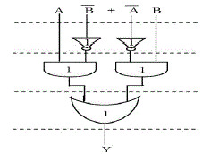
| The AND, OR, and Inverter (AOI) implementation of an XOR gate is shown in Fig. 1. The gates between the dotted lines are performing the operations in parallel and the numeric representation of each gate indicates the delay contributed by that gate. |
| The delay and area evaluation methodology considers all gates to be made up of AND, OR, and Inverter, each having delay equal to 1 unit and area equal to 1 unit. We then add up the number of gates in the longest path of a logic block that contributes to the maximum delay. The area evaluation is done by counting the total number of AOI gates required for each logic block. Based on this approach, the CSLA adder blocks of 2:1 mux, Half Adder (HA), and FA are evaluated and listed in Table I. |
BEC
|
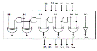
| As stated above the main idea of this work is to use BEC instead of the RCA with Cin=1 in order to reduce the area and power consumption of the regular CSLA. To replace the n-bit RCA, an n+1-bit BEC is required. A structure of a 6-b BEC are shown in Fig. 2 . |
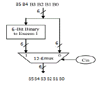
| Fig. 3 illustrates how the basic function of the CSLA is obtained by using the 6-bit BEC together with the mux. One input of the 12:6 mux gets as it input (B5,B4,B3, B2, B1, and B0) and another input of the mux is the BEC output. This produces the two possible partial results in parallel and the mux is used to select either the BEC output or the direct inputs according to the control signal Cin. The importance of the BEC logic stems from the large silicon area reduction when the CSLA with large number of bits are designed. The Boolean expressions of the 6-bit BEC is listed as (note the functional symbols ~ NOT,&AND,^XOR) |
| X0 = ~B0 |
| X1 = B0^B1 |
| X2 = B2^ (B0 & B1) |
| X3 = B3^ (B0 & B1 & B2) |
| X4 = B4^ (B0 & B1 & B2 & B3) |
| X5 = B5^ (B0 & B1 & B2 & B3 & B4). |
DELAY AND AREA EVALUATION METHODOLOGY OF REGULAR 128-B SQRT CSLA
|
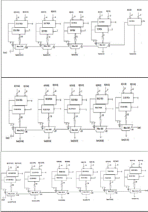
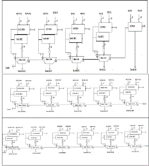
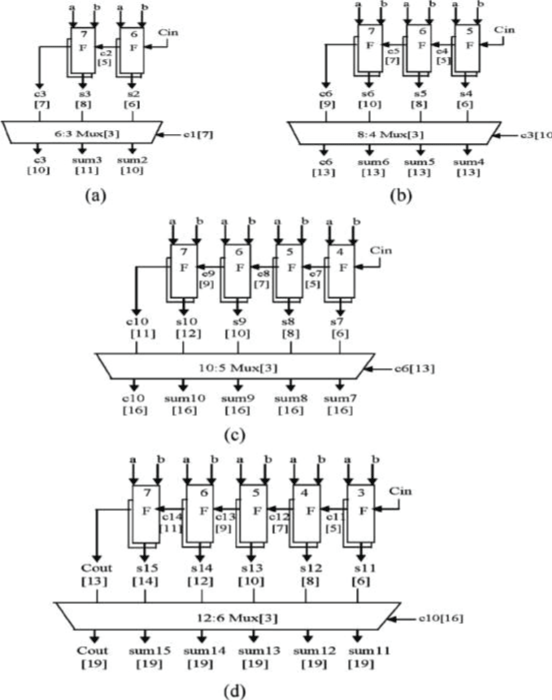
| The structure of the 128-b regular SQRT CSLA is shown in Fig. 4. It has sixteen groups of different size RCA. The delay and area evaluation of first five groups are shown in Fig. 5, in which the numerals within [ ] specify the delay values, e.g., sum2 requires 10 gate delays. The steps leading to the evaluation are as follows. |
| 1) The group2 [see Fig. 5(a)] has two sets of 2-b RCA. Based on the consideration of delay values of Table I, the arrival time of selection input c1[time(t)=7] of 6:3 mux is earlier than S3[t=8] and later than s2[t =6] Thus, sum3[t = 11] is summation of S3 and MUX[t=3] andSUM2[t=10] is summation of C1 and mux. |
| 2) Except for group2, the arrival time of mux selection input is always greater than the arrival time of data outputs from the RCA’s. Thus, the delay of group3 to group5 is determined, respectively as follows: |
| {c6; sum[6 : 4]} = c3[t =10]+mux |
| {c10; sum[10 : 7]} = c6[t = 13] + mux |
| {cout; sum[15 : 11]} = c10[t = 16] + mux. |
| 3) The one set of 2-b RCA in group2 has 2 FA for Cin=1and the other set has 1 FA and 1 HA for Cin=0. Based on the area count of Table I, the total number of gate counts in group2 is determined as follows: |
| Gate count=57(FA+HA+MUX). |
| FA=39(3 *13) |
| HA=6(1 * 6) |
| Mux=12(3* 4) |
| 4) Similarly, the estimated maximum delay and area of the other groups in the regular SQRT CSLA are evaluated. |
DELAY AND AREA EVALUATION METHODOLOGY OF MODIFIED128-B SQRT CSLA
|
| The structure of the proposed 128-b SQRT CSLA using BEC for RCA with Cin =1 to optimize the area and power is shown in Fig. 6. We again split the first16-bits from the structure into five groups. The delay and area estimation of each group are shown in Fig. 7. The steps leading to the evaluation are given here. |
| 1) The group2 [see Fig. 7(a)] has one 2-b RCA which has 1 FA and 1 HA for Cin=0 Instead of another 2-b RCA with Cin =1 a 3- b BEC is used which adds one to the output from 2-b RCA. |
| Based on the consideration of delay values of Table I, the arrival time of selection input C1[time(t)=7] of 6:3 mux is earlier than the S3[t=9]and C3[t=10]and later than the S2[t=4]Thus, the sum3 and final C3 (output from mux) are depending on S3 and mux and partial C3 (input to mux) and mux, respectively. The sum2 depends on C1 and mux. |
| 2) For the remaining group’s the arrival time of mux selection input is always greater than the arrival time of data inputs from the BEC’s. Thus, the delay of the remaining groups depends on the arrival time of mux selection input and the mux delay. |
| 3) the area count of group 2 is determined as follows : |
| Gate count = 43(FA+HA+MUX+BEC) |
| FA=13(1*13) |
| HA=6(1*6) |
| AND = 1 |
| NOT = 1 |
| MUX =12(3*4) |
| XOR = 10(2*5). |
| 4)Similarly, the estimated maximum delay and area of the other groups of the modified SQRT CSLA are evaluated. this SQRT CSLA saves 113 gate areas than the regular SQRT CSLA, with only 11 increases in gate delays. To further evaluate the performance, we have resorted to ASIC implementation and simulation. |
ASIC IMPLEMENTATION RESULTS
|
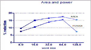
| The design proposed in this paper has been developed using Verilog- HDL and synthesized in Cadence RTL compiler using typical libraries of TSMC 0.18 um technology. The synthesized Verilog netlist and their respective design constraints file (SDC) are imported to Cadence SoC Encounter and are used to generate automated layout from standard cells and placement and routing [7]. Parasitic extraction is performed using Encounter’s Native RC extraction tool and the extracted parasitic RC (SPEF format) is back annotated to Common Timing Engine in Encounter platform for static timing analysis. For each word size of the adder, The similar design flow is followed for both the regular and modified SQRT CSLA. Table II exhibits the simulation results of both the CSLA structures in terms of delay, area and power. The area indicates the total cell area of the design and the total power is sum of the leakage power, internal power and switching power. The percentage reduction in the cell area, total power, power-delay product and the area–delay product as function of the bit size are shown in Fig. 8(a). Also plotted is the percentage delay overhead in Fig. 8(b). It is clear that the area of the 8-, 16-, 32-, 64-,128-b proposed SQRT CSLA is reduced by 9.7%, 15%, 16.7%, and 17.4%, respectively. The total power consumed shows a similar trend of increasing reduction in power consumption 7.6%, 10.56%, 13.63%,and 15.46 % with the bit size. Interestingly, the delay overhead also exhibits a similarly decreasing trend with bit size. The delay overhead for the 8, 16, and 32-b is 14%, 9.8%, and 6.7% respectively, whereas for the 64-b it reduces to only 3.76%. The power–delay product of the proposed 8-b is higher than that of the regular SQRT CSLA by 5.2% and the area-delay product is lower by 2.9%. However, the power-delay product of the proposed 16-b SQRT CSLA reduces by 1.76% and for the 32-b and 64-b by as much as 8.18%, and 12.28% respectively. Similarly the area-delay product of the proposed design for 16-, 32-, and 64-b is also reduced by 6.7%, 11%, and 14.4% respectively . |
CONCLUSION
|
| A simple approach is proposed in this paper to reduce the area and power of SQRT CSLA architecture. The reduced number of gates of this work offers the great advantage in the reduction of area and also the total power. The compared results show that the modified SQRT CSLA has a slightly larger delay (only 3.76%), but the area and power of the 64-b modified SQRT CSLA are significantly reduced by 17.4% and 15.4% respectively. |
| The power-delay product and also the area-delay product of the proposed design show a decrease for 16-, 32-, and 64-b sizes which indicates the success of the method and not a mere tradeoff of delay for power and area. The modified CSLA architecture is therefore, low area, low power, simple and efficient for VLSI hardware implementation It would be interesting to test the design of the modified 128-b SQRT CSLA. |
Tables at a glance
|
 |
 |
| Table 1 |
Table 2 |
|
| |
Figures at a glance
|
 |
 |
 |
 |
| Figure 1 |
Figure 2 |
Figure 3 |
Figure 4 |
 |
 |
 |
 |
| Figure 5 |
Figure 6 |
Figure 7 |
Figure 8 |
|
| |
References
|
- O. J. Bedrij, “Carry-select adder,” IRE Trans. Electron. Comput., pp. 340–344, 1962.
- B. Ramkumar, H.M. Kittur, and P. M. Kannan, “ASIC implementation of modified faster carry save adder,” Eur. J. Sci. Res., vol. 42, no. 1, pp. 53–58,2010.
- T. Y. Ceiang and M. J. Hsiao, “Carry-select adder using single ripple carry adder,” Electron. Lett., vol. 34, no. 22, pp. 2101–2103, Oct. 1998.
- Y. Kim and L.-S. Kim, “64-bit carry-select adder with reduced area,” Electron. Lett., vol. 37, no. 10, pp. 614–615, May 2001.
- J. M. Rabaey,Digtal Integrated Circuits—A Design Perspective. Upper Saddle River, NJ: Prentice-Hall, 2001.
- Y. He, C. H. Chang, and J. Gu, “An area efficient 64-bit square root carry-select adder for low power applications,” in Proc. IEEE Int. Symp. Circuits Syst., 2005, vol. 4, pp. 4082–4085.
- Cadence, “Encounter user guide,” Version 6.2.4, March 2008.
|