Keywords
|
| Amplitude modulation (AM), dc-ac power conversion, harmonic control, HVDC, insulated-gate bipolar transistor (IGBT), power electronics, power transmission system, pulse-width modulation, voltage-source converter (VSC). |
INTRODUCTION
|
| The continuous growth of electricity demand and ever increasing society awareness of climate change issues directly affect the development of the electricity grid infrastructure. The utility industry faces continuous pressure to transform the way the electricity grid is managed and operated. On one hand, the diversity of supply aims to increase the energy mix and accommodate more and various sustainable energy sources. On the other hand, there is a clear need to improve the efficiency, reliability, energy security, and quality of supply. With the breadth of benefits that the smart grid can deliver, the improvements in technology capabilities, and the reduction in technology cost, investing in smart grid Technologies has become a serious focus for utilities [1]. |
| Advanced technologies, such as flexible alternating current transmission system (FACTS) and voltage-source converter (VSC)-based high-voltage dc (HVDC) power transmission systems, are essential for the restructuring of the power systems into more automated, electronically controlled smart grids. An overview of the recent advances of HVDC based on VSC technologies is offered in [2]. The most important control and modeling methods of VSC-based HVDC systems and the list of existing installations are also available in [2] |
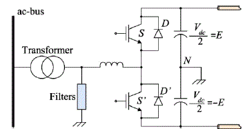
| The first generation of utility power converters is based on current-source converter (CSC) topologies [3], [4]. Today, many projects still use CSCs due to their ultra-high power capabilities. With the invention of fully controlled power semiconductors, such as insulated-gate bipolar transistors (IGBTs) and integrated gate-commutated thyristors (IGCTs) [5], the VSC topologies are more attractive due to their four-quadrant power-flow characteristics [6]. A typical configuration of the VSC-based HVDC power transmission system is shown in Fig. 1 as it is shown in [7] and [8]. |
| With the continued increase of power and voltage levels, stress on cost effective solutions and stringent guidelines for power quality, multilevel converters have emerged as a technically viable solution for accomplishing acceptable standards. The term âÃâ¬ÃâMultilevel‘ has been coined to emphasize the ability to increase the instantaneous voltage levels in steps, accomplished by addition of components in series. The basic topologies that have been studied so far are namely: Diode Clamped, Flying Capacitor, Cascaded H-bridge and the Modular Topology. Although the different topologies offer a variety of advantages, they however, also possess some limitations with further increase in voltage levels.. |
| Additionally, due to its modular structure, the hardware implementation is rather simple and the maintenance operation is easier than alternative multilevel converters. The multilevel voltage source inverter is recently applied in many industrial applications such as ac power supplies, static VAR compensators, drive systems, etc. One of the significant advantages of multilevel configuration is the harmonic reduction in the output waveform without increasing switching frequency or decreasing the inverter power output [5-11]. The output voltage waveform of a multilevel inverter is composed of the number of levels of voltages, typically obtained from capacitor voltage sources. The so-called multilevel starts from three levels. As the number of levels reach infinity, the output THD approaches zero. The number of the achievable voltage levels, however, is limited by voltage unbalance problems voltage clamping requirement, circuit layout, and packaging constraints. |
| On the other hand, optimized modulation methods offer many advantages toward tight control of converter-generated harmonics [19]. A minimization method to find the complete set of solutions by solving the SHE-PWM equations for twolevel inverters is discussed in [20]. In this paper, the dc-link voltage is assumed to be constant. In [10], a method is proposed to prevent the dc-link ripple voltage from creating low-order harmonics on the ac side of fixed and variable frequency inverters. However, only one of the multiple SHE-PWM sets [20] of solutions is reported. |
| An investigation of the harmonic interaction between the ac and dc side for STATCOM is presented in [21] including the so-called dynamic SHE-PWM scheme based on pre calculated angles for better THD. However, the dynamic SHE-PWM scheme is applied only for a three-level converter and can be applied only for known magnitude and frequency of the ripple. Another method for improving the harmonic performance of a two-level VSC with SHE-PWM is studied in [22]. However, only one set of SHE-PWM solutions is considered for the method of [22] which requires the exact values of magnitude, phase, and frequency of the ripple in order to be implemented. |
| Control strategies to compensate unbalances are reported in the literature. Mild imbalances caused by unbalanced loads of the ac side are regulated by using separate control loops for the positive- and negative-sequence components of the voltage as proposed in [23]. Efficient control of unbalanced compensator currents can be achieved by a control algorithm based on the D-STATCOM model [24]. D-STATCOM allows separate control of positive- and negative-sequence currents and decoupled current control of the d-q frame. An advanced strategy based on direct power control under unbalanced grid voltage conditions has been recently presented for a doubly fed induction generator [25]. To take the full advantages of VSCs for HVDC power transmission systems, an auxiliary controller is added to the main controller which is conventionally implemented in the positive-sequence d-q frame [26]. To compensate for unbalanced ac-side loads, the auxiliary controller is implemented in the negative-sequence d-q frame. |
| The objective of this paper is to discuss the effectiveness of optimized modulation based on pre-calculated SHE-PWM in a two-level three-phase VSC to make the ac side immune from the fluctuations of the dc link without the use of passive components. However, since the VSC studied here does not include a closed-loop controller, strategies to compensate unbalances are not addressed in this paper. |
| This paper is organized in the following way. In Section II, a brief analysis of the VSC and the modulation method is provided. Section III contains the characteristics of the method on a VSC with dc-side ripple voltage. Section IV provides extensive experimental results to support the theoretical arguments. Conclusions are documented in Section V. |
ANALYSIS OF THE PWM CONVERTER AND SHE-PWM
|
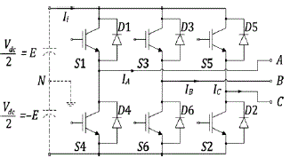
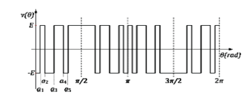
| The optimized SHE-PWM technique is investigated on a two level three-phase VSC topology with IGBT technology, shown in Fig. 2. A typical periodic two-level SHE-PWM waveform is shown in Fig.3. The waveforms of the line-to-neutral voltages can be expressed as follows: |
 |
| When ω0 is the operating frequency of the ac, and |
| Vdc is the dc-link voltage. |
| Thus, the line-to-line voltages are given by |
 |
| The SHE-PWM method offers numerical solutions which are calculated through the Fourier series expansion [20] of the waveform |
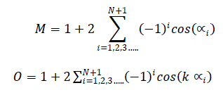 |
| Where N+1 are the angles that need to be found. |
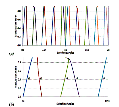
| Using five switching angles per quarter-wave in (N=4)SHE-PWM, k= 5, 7, 11, 13 to eliminate the 5th, 7th, 11th,and 13th harmonics. During the case of a balanced load, the third and all other harmonics that are multiples of three are cancelled, due to the 120 symmetry of the switching function of the three-phase converter. The even harmonics are cancelled due to the half-wave quarter-wave symmetry of the angles, being constrained by |
| 0 < α1 < α2 … … .< αN+1 < π/ 2 |
Diode Clamped Multilevel Converter
|
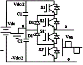
| Table I shows the switching states of the 3-level Diode clamped multilevel inverter with the switching states of V0, 0 and - Vdc |
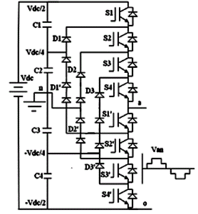
| Fig.7 shows the circuit diagram of the 5-level Diode clamped multilevel inverter |
| Table II shows the switching states of the Diode clamped multilevel inverter. |
SIMULATION RESULTS
|
| Modeling of Diode Clamped Multilevel Converter |
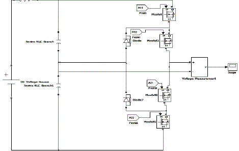
| Fig.8 shows the Matlab/Simulink Model of three level Diode clamped multilevel converter. |
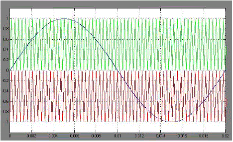
| Fig.9 shows the Level shifted Carrier PWM wave form. Here two carriers each are level shifted and are compared with sine wave. |
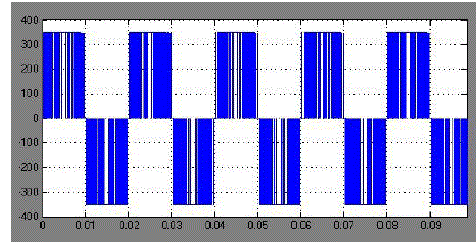
| Fig.10 shows the three level output voltage waveform. |
| Case 2 |
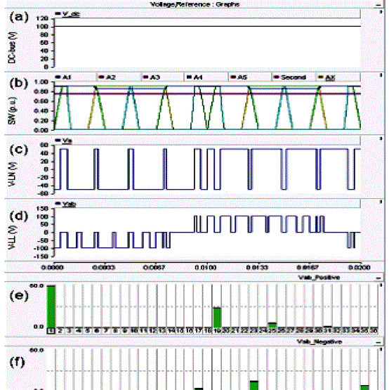
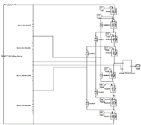
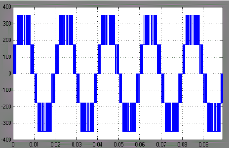
| Fig.11 shows the Matlab/Simulink Model of five level Diode clamped multilevel converter. |
| Fig.11 shows the Level shifted Carrier PWM wave form. Here four carriers each are level shifted and are compared with sine wave. |
| Fig.12 shows the five level output voltage waveform of the diode clamped multilevel inverter. |
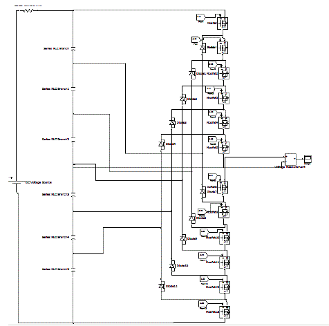
| Fig.13 shows the simulink model of the Seven level diode clamped multilevel inverter. |
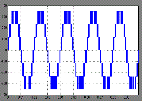
| Fig.13 shows the Level shifted Carrier PWM wave form. Here four carriers each are level shifted and are compared with sine wave. |
| Fig.14 shows the five level output voltage waveform of the diode clamped multilevel inverter |
CONCLUSION
|
| This paper presents Diode Clamped multilevel converter. The three-level converter using the modular topology was simulated for the same voltage and power rating as the two-level converter. With higher levels, the use of PWM does not offer significant benefit as we have increased losses hence, SHE modulation strategy was utilized and the results were compared for increasing delay angles. For the same power and voltage rating, higher levels of the modular topology, were also simulated. Higher levels, implies the use of more number of submodules to generate intermediate steps in the instantaneous voltage wave to make it more sinusoidal. Finally a seven level single H-bridge is proposed. A SIMULINK based model is developed and Simulation results are presented. |
Tables at a glance
|
 |
 |
| Table 1 |
Table 2 |
|
Figures at a glance
|
 |
 |
 |
 |
 |
| Figure 1 |
Figure 2 |
Figure 3 |
Figure 4 |
Figure 5 |
 |
 |
 |
 |
 |
| Figure 6 |
Figure 7 |
Figure 8 |
Figure 9 |
Figure 10 |
 |
 |
 |
 |
| Figure 11 |
Figure 12 |
Figure 13 |
Figure 14 |
|
References
|
- J. McDonald, âÃâ¬Ãâ¢Leader or follower The business scene],âÃâ¬Ãâ IEEE Power Energy Mag., vol. 6, no. 6, pp. 18–90, Nov. 2008.
- N. Flourentzou, V. G. Agelidis, and G. D. Demetriades, âÃâ¬Ãâ¢VSC-based HVDC power transmission systems: An overview,âÃâ¬Ãâ IEEE Trans. PowerElectron., vol. 24, no. 3, pp. 592–602, Mar. 2009.
- A. Edris, S. Zelingher, L. Gyugyi, and L. J. Kovalsky, âÃâ¬Ãâ¢Squeezing more power from the grid,âÃâ¬Ãâ IEEE Power Eng. Rev., vol. 22, no. 6, pp. 4–6,Jun. 2002.
- K. Perkins and M. R. Iravani, âÃâ¬Ãâ¢Dynamic modeling of high power static switching circuits in the dq-frame,âÃâ¬Ãâ IEEE Trans. Power Syst., vol. 14, no. 2,pp. 678–684, May 1999.
- P. Steimer, O. Apeldoorn, E. Carroll, and A. Nagel, âÃâ¬Ãâ¢IGCT technology baseline and future opportunities,âÃâ¬Ãâ in Proc. IEEE Transmi. Distrib. Conf.Expo., Oct. 2001, vol. 2, pp. 1182–1187.
- V. G. Agelidis and G. Joos, âÃâ¬Ãâ¢On applying graph theory toward a unified analysis of three-phase PWM inverter topologies,âÃâ¬Ãâ in Proc. IEEE PowerElectronics Specialists Conf., Seattle, WA, Jun. 1993, pp. 408–415.
- J. Arrillaga, Y. H. Liu, and N. RWatson, Flexible Power Transmission: The HVDC options. Hoboken, NJ: Wiley, 2007.
- G. Asplund, âÃâ¬Ãâ¢Application of HVDC light to power system enhancement,âÃâ¬Ãâin Proc. IEEE Power Eng. Soc. Winter Meeting, Singapore, Jan. 2000, vol.4, pp. 2498–2503
- P. N. Enjeti, P. D. Ziogas, and M. Ehsani, âÃâ¬Ãâ¢UnbalancedPWMconverter analysis and corrective measures,âÃâ¬Ãâ in Proc. IEEE Industry Applications Soc.Annu. Meet., San Diego, CA, Oct. 1989, pp. 861–870.
- P. N. Enjeti and W. Shireen, âÃâ¬Ãâ¢A new technique to reject dc-link voltage ripple for inverters operating on programmedPWM waveforms,âÃâ¬Ãâ IEEE Trans.Power Electron., vol. 7, no. 1, pp. 171–180, Jan. 1992.
- J. Y. Lee and Y. Y. Sun, âÃâ¬Ãâ¢Adaptive harmonic control in PWM inverters with fluctuating input voltage,âÃâ¬Ãâ IEEE Trans. Ind. Electron., vol. IE-33, no. 1,pp. 92–98, Feb. 1986.
- S. Funabiki and Y. Sawada, âÃâ¬Ãâ¢Computative decision of pulse width in three-phase PWM inverter,âÃâ¬Ãâ in Proc. IEEE Industry Applications Soc. Annu.Meet., Pittsburgh, PA, Oct. 1988, pp. 694–699.
- T. Kato, âÃâ¬Ãâ¢Precise PWM waveform analysis of inverter for selected harmonic elimination,âÃâ¬Ãâ in Proc. IEEE Industry Appl. Soc. Annu. Meeting,Piscataway, NJ, Sep. 1986, vol. 1, pp. 611–616.
- B. P. McGrath and D. G. Holmes, âÃâ¬Ãâ¢A general analytical method for calculating inverter dc-link current harmonics,âÃâ¬Ãâ in Proc. IEEE Ind. Appl. Soc.Annu. Meeting, Edmonton, AB, Canada, Oct. 2008, pp. 1–8.
- A. M. Cross, P. D. Evans, and A. J. Forsyth, âÃâ¬Ãâ¢DC link current in PWMinverters with unbalanced and nonlinear loads,âÃâ¬Ãâ Proc. Inst. Elect. Eng., Elect. Power Appl., vol. 146, no. 6, pp. 620–626, Nov. 1999.
- M. H. Bierhoff and F. W. Fuchs, âÃâ¬Ãâ¢DC-link harmonics of three-phase voltage-source converters influenced by the pulsewidth-modulation strategy—An analysis,âÃâ¬Ãâ IEEE Trans. Ind. Electron., vol. 55, no. 5, pp. 2085–2092, May 2008.
- M. N. Anwar and M. Teimor, âÃâ¬Ãâ¢An analytical method for selecting dc-link-capacitor of a voltage stiff inverter,âÃâ¬Ãâ in Proc. 37th IAS Annu.MeetingIEEE Industry Applications Conf., Dearborn, MI, Oct. 2002, vol. 2, pp. 803–810.
- F. D. Kieferndorf, M. Forster, and T. A. Lipo, âÃâ¬Ãâ¢Reduction of dc-bus capacitor ripple current with PAM/PWM converter,âÃâ¬Ãâ IEEE Trans. Ind. Appl.,vol. 40, no. 2, pp. 607–614, Mar. 2004.
- P. N. Enjeti, P. D. Ziogas, and J. F. Lindsay, âÃâ¬Ãâ¢Programmed PWM techniques to eliminate harmonics: A critical evaluation,âÃâ¬Ãâ IEEE Trans. Ind.Appl., vol. 26, no. 2, pp. 302–316, Mar. 1990.
- V. G. Agelidis, A. Balouktsis, I. Balouktsis, and C. Cossar, âÃâ¬Ãâ¢Multiple sets of solutions for harmonic elimination PWM bipolar waveforms:Analysis and experimental verification,âÃâ¬Ãâ IEEE Trans. Power Electron., vol. 21, no. 2, pp. 415–421, Mar. 2006.
- L. Ran, L. Holdsworth, and G. A. Putrus, âÃâ¬Ãâ¢Dynamic selective harmonic elimination of a three-level inverter used for static VAr compensation,âÃâ¬ÃâProc. Inst. Elect. Eng., Gen., Transm. Distrib., vol. 149, no. 1, pp. 83–89, Jan. 2002.
- 2 S. Filizadeh and A. M. Gole, âÃâ¬Ãâ¢Harmonic performance analysis of an OPWM-controlled STATCOM in network applications,âÃâ¬Ãâ IEEE Trans. PowerDel., vol. 20, no. 2, pt. 1, pp. 1001–1008, Apr. 2005.
- C. Hochgraf and R. H. Lasseter, âÃâ¬Ãâ¢Statcom controls for operation with unbalanced voltages,âÃâ¬Ãâ IEEE Trans. Power Del., vol. 13, no. 2, pp. 538–544,Apr. 1998.
- B. Blazic and I. Papic, âÃâ¬Ãâ¢Improved D-STATCOM control for operation with unbalanced currents and voltages,âÃâ¬Ãâ IEEE Trans. Power Del., vol. 21, no.1, pp. 225–233, Jan. 2006.
- D. Santos-Martin, J. L. Rodriguez-Amenedo, and S. Arnalte, âÃâ¬Ãâ¢Direct power control applied to doubly fed induction generator under unbalanced gridvoltage conditions,âÃâ¬Ãâ IEEE Trans. Power Electron., vol. 23, no. 5, pp. 2328–2336, Sep. 2008.
- L. Xu, B. R. Andersen, and P. Cartwright, âÃâ¬Ãâ¢VSC transmission operating under unbalanced AC conditions—Analysis and control design,âÃâ¬ÃâIEEETrans. Power Del., vol. 20, no. 1, pp. 427–434, Jan. 2005.
- IEEE Recommended Practice for Electric Power Distribution for Industrial Plants, IEEE Std. 141-1993, 1994.
- N. Flourentzou and V. G. Agelidis, âÃâ¬Ãâ¢Harmonic performance of multiple sets of solutions of SHE-PWM for a two-level VSC topology withfluctuating dc-link voltage,âÃâ¬Ãâ in Proc. Australasian Universities Power Eng. Conf., Perth, WA, Australia, Dec. 2007, pp. 511–518.
|