Current source drivers (CSDs) have been reduce the switching loss and gate drive loss in megahertz (MHz) dc-dc converters, in which the duty cycle normally has a steady-state value. However, different from dc-dc converters, the duty cycle of the power factor correction (PFC) converters is modulated fast and has a wide operating range during a half-line period in ac –dc applications. An adaptive full-bridge CSD is used as a boost PFC converters. The CSD can build adaptive drive current inherently depending on the drain current of the main power MOSFET. Compared to the CSDs with the constant drive current, the advantage of the adaptive drive current is reduce the switching loss further when the MOSFET is with a higher switching current, while minimizing the drive circuit loss when the MOSFET is with a lower switching current. Therefore, the adaptive CSD is able to realize better design tradeoff between the switching losses and drive circuit loss so that the efficiency can be optimized in a wide operation range. Furthermore, no additional auxiliary circuit and control are needed to realize the adaptive current. A full bridge (FB) inverter at the back end of dc-dc converter completes the ac-ac conversion. This circuit enables to provide controlled and regulated ac output. The AC-AC converter is designed and simulated using MATLAB 2010 and waveforms are analysied. Simulation results demonstrate that the output voltage of the desired converter can be maintained at 349 V ac and Power factor can be improvedupto 0.909.
Keywords |
| Interleaved Boost Converter (IBC), Current Source Driver (CSD), Power MOSFET, Power Factor
Correction (PFC), Inverter |
INTRODUCTION |
| An adaptive FB CSD for boost PFC converters to achieve fast switching speed and significant switching loss reduction.
Compared to other CSDs with the constant drive current, the advantage of the adaptive drive current is reduce
switching loss further when the power MOSFET is with a higher switching current, while reducing drive circuit loss
when the MOSFET is with a lower switching current. This provides better optimal opportunity with the trade-off
between the switching loss reduction and CSD drive circuit loss during a wide operation range [1]. Compared to the
Resonate gate drives and CSDs can not only recover the excessive gate drive loss but also reduce the dominant
switching losses in hard switching converters. An Interleaved PFC boost converter simply consists of two body
converter in parallel operation 1800 out of phase. It is used to increase the conversion energy and power conversion
density and reduce ripple amplitude. The advantage of interleaved boost converter compared to the classical boost
converter are low input current ripple, high efficiency, and faster transient response, reduced electromagnetic emission
and improved reliability. The Interleaved boost converter has high voltage step up, reduced voltage ripple at the output,
low switching losses, reduced electromagnetic interference and faster transient response. Also, the steady-state voltage
ripples at the output capacitors of IBC are reduced [2]. Though IBC topology has more inductors increasing the
complexity of the converter compared to the conventional boost converter it is preferred because of the low ripple
content in the input and output sides. In order to reduce this complexity, this suitable IBC for both fuel cell and PV
applications. In ac–dc applications, the power factor correction (PFC) technique is widely used. Different from dc–dc
converters, the duty cycle of the PFC converters needs to be modulated fast and has a wide operation range. Normally,
the switching loss is proportional to the switching current and the drain-to-source voltage. For a boost PFC converter, the input line current follows the input line voltage in the same phase. When the line voltage reaches the peak value of
the power MOSFET, the line current also reaches the peak and so does the drain This means that the switching loss
reaches its maximum value at this moment. Output of dc-dc converter fed to single phase Full Bridge Inverter [3]. The
frequency of output voltage can be controlled by varying the time period. The switching signals of full bridge inverter
provided by using Sinusoidal Pulse Width Modulation (SPWM). Working of the circuit and verification by simulation
results are discussed in this paper. Simulation is done in MATLAB 2010 with 110 Vac input and output is 349 Vac
output. |
CSD FOR A BOOST CONVERTER |
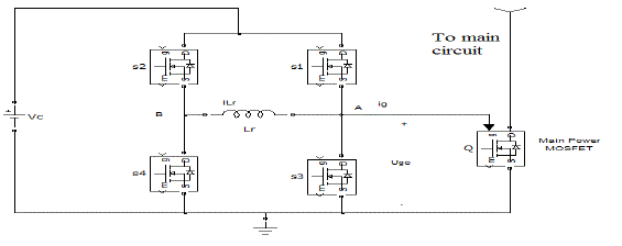
| The CSD circuit for the boost PFC converter is shown in Figure 2. Compared to half bridge CSD switch S2 and S4 are
used to remove the blocking capacitor Cb, which forms a Full Bridge (FB) CSD structure [4]. Since there is no longer
any blocking capacitor Cb, the CSD is be suitable for the boost PFC converters with the modulated duty cycle. It
consists of four switches S1 and S3, and S2 and S4 are controlled complementarily with dead time. |
| A. Principle of Operation |
| The CSD circuit for PFC application is shown in Figure 3. It consist body diodes D1-D4 and capacitors C1-C4 are the
drain-to-source capacitance which are connected across the S1-S4, respectively Cgs is the gate-to-source capacitor of Q.
Thereare eight switching modes in one switching period. |
| 1) Mode -1:If S3 is on and the gate of Q is clamped to ground. When S3 is turned off, the peak value Ipeak of the
inductor current ILr charges C3 plus Cgs and dischargeC1through the Current Source (CS). Due to C1 and C3, S3 achieves
zero-voltage turnoff. The voltage of C3 rises linearly and the voltage of C1 decays linearly. |
| 2) Mode -2:The body diode D1 conducts and S1turned ON with the zero-voltage condition. The gate-to-source voltage
of Q is clamped to Vc through S1. During this interval, ILr decreases and changes its polarity from Ipeak to -Ipeak. |
| 3) Mode -3: If S1turned OFF and the negative peak value -Ipeak charges C1 and discharges C3 plus Cgsthrough the as a
CS. Due to C1 and C3, S1 achieves zero-voltage turnoff. Then the voltage of C1 rises and the voltage of C3 decreases
linearly |
| 4) Mode -4:If D3 conducts and S3turned ON with the zero-voltage condition. The gate to- source voltage of Q is
clamped to ground through S3. The current path during this interval is S3–Lr –S4. ILr circulates through S3 and S4 and
remains constant in this interval. |
| 5) Mode -5:If S4turned OFF and the negative peak current -Ipeak charges C4 and discharges C2through the. Due to C2
and C4, S4 achieves zero voltage turnoff. The voltage of C4 rises linearly and the voltage of C2 decays linearly. |
| 6) Mode -6:If D2 conducts and S2turned ON with the zero-voltage condition. ILr decreases from -Ipeak and changes its
polarity to Ipeak. |
| 7) Mode -7:If S2turned OFF. The peak drive current Ipeak charges C2 and discharges C4. The voltage of C2 rises
linearly and the voltage of C4 decays linearly. |
| 8) Mode -8:IfD4 conducts and S4turned ON with the zero-voltage condition. The current path during this interval is S4–
Lr –S3. ILr circulates through S3 and S4 and remains constant during this interval [1]. |
| B. Adaptive Gate Drive Current of Power MOSFET |
| In mode 2, the voltage applied to the inductor VAB is the drive voltage Vc. The relationship between the inductor value |
| Lr and the peak current Ipeak of the Current Source inductor is |
 |
 |
| Where D is the duty ratio, f is the frequency and Lris the inductor.Advantages of adaptive current source drives are
overall efficiency can achieve during a wide operation range, leads to a higher driver current, faster switching speed
andlower switching loss. |
INTERLEAVING BOOST PFC CONVERTERS WITH CSD |
| The presented adaptive CSD circuit with one inductor can drive two interleaved boost PFC converters directly as
shown in Figure 4. The advantage is that only single FB CSD is required. It is noted that Q1 and Q2 are turned ON and
OFF by the peak current of the CS inductor so that fast switching speed and switching loss reduction can be realized. In
addition, S1, S3 and S2, S4 are with complementary control, respectively, and therefore, the commercial buck drivers
with two complementary drive signals can be directly used to the CSD circuit. These reduce the complexity of the CSD
circuit implementation with the discrete components. Other benefits of this topology include low current stress of the
power MOSFETs, ripple cancellation of input current and reduced boost inductances. |
INVERTER TOPOLOGY |
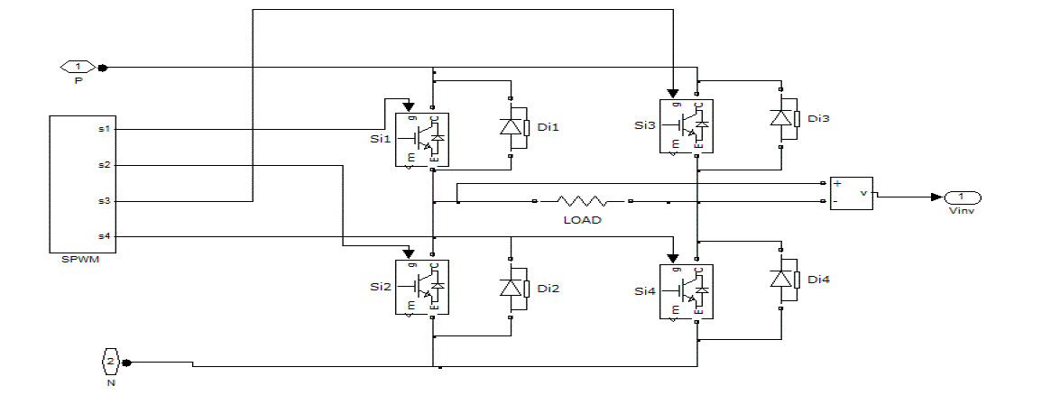
| Figure 6 shows the power diagram of the single phase full bridge inverter. The inverter uses two pairs of controlled
switches (T1, T4 and T2, T3) and two pairs of diodes (D1, D4 and D2, D3). The devices of one pair operate
simultaneously. In order to develop a positive voltage (+Vb) across load, switches T1 and T4 are tuned-on
simultaneously whereas to have a negative voltage (-Vb) across load, we need to turn-on the switches T2 and T3. Diodes
D1, D2, D3 and D4 are known as feedback diodes [5] |
SIMULINK MODEL |
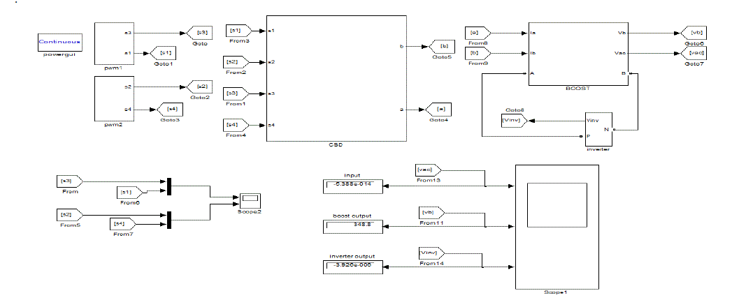
| The main Simulink model of the system is shown in Figure 6. It consists of five subsystems. These subsystems are
PWM-1, PWM-2, CSD, BOOST and INVERTER circuit model, and output signal is connected into scope. The output
scope shows input voltage, boost voltage and inverter voltage across load. |
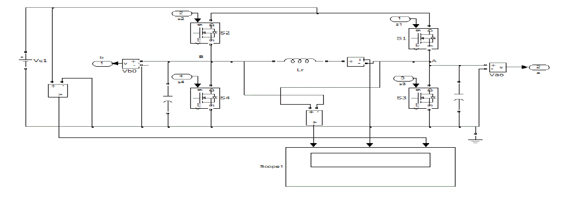
| The CSD model of system is shown in Figure 7. It consists of four MOSFET and current source inductor Lr connected
between the point A and B. Here Lr is 1:5��H and drive voltage is 12V. |
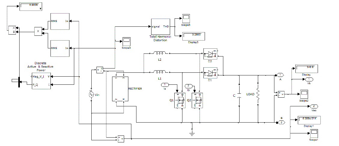
| The Interleaving Boost model of the system is shown in Figure 8. It consists of two switches Q1 and Q2that are
connected in parallel with the same reference node, and two inductors L1 and L2.Here L1 and L2 are equal, and diodes
are connected in parallel with each other. Boost inductor is 100��F and capacitor is 220��F. Gate signal of Q1 and Q2 are
coming from the CSD. |
| The Inverter model of the system is shown in Figure 9. It consists of four switches and four diodes that are connected in
anti-parallel for feedback. Unipolar SPWM are used for working of switch. |
SIMULATION RESULTS AND ANALYSIS |
| For the adaptive CSD, Drive Voltage is 12 V and source current inductor Lr is 1.5��H. The input voltage is 110 Vac and
the output is 349 Vac. The specifications for boost inductor L = 100 μH; output capacitance C = 220 μF. Figure 10(a) is
the input voltage with 110Vac with 50Hz frequency. The input ac voltage gets converted by rectifier and then fed toa
DC-DC boost converter to get the required voltage level of 349V and it is shown in Figure 10(b). This boosted voltage
is inverted into ac voltage by full bridge inverter. Figure 10(c) is output of inverter ac voltage with 349Vac |
| For the adaptive CSD, Drive Voltage is 12 V and source current inductor Lr is 1:5��H. The output of the CSD model of
voltage across the source inductor is shown in Figure 11(a). The output of the current through the current source
inductor ILpeakis shown in Figure 11(b).The switches S1S2S3 and S4 are fed to the CSD. These switches are shown in
Figure 12 (a) and Figure 12 (b). |
CONCLUSIONS |
| An adaptive FB CSD for boost PFC converters to achieve fast switching speed and significant switching loss reduction.
The advantage of the adaptive drive current can achieve further switching loss reduction when the power MOSFET is
with a higher switching current while reduce the circuit loss when the MOSFET is with a lower switching current. A
full bridge inverter at the back end of dc-dc converter completes the ac-ac conversion. This circuit enables to provide
controlled and regulated ac output. The simulation results highlights the work done to maintain the output voltage of
the converter 349 Vac the circuit parameter enhance the power factor upto0.909[6]. |
Figures at a glance |
 |
 |
 |
 |
| Figure 1 |
Figure 2 |
Figure 3 |
Figure 4 |
 |
 |
 |
 |
| Figure 5 |
Figure 6 |
Figure 7 |
Figure 8 |
 |
 |
 |
 |
| Figure 9 |
Figure 10 |
Figure 11 |
Figure 12 |
|
References |
- Zhiliang Zhang, Member, IEEE, PengchengXu, and Yan-Fei Liu, Senior Member, IEEE ” Adaptive Continuous Current Source Drivers for 1- MHz Boost PFC Converters ”IEEE Transactions On Power Electronics, Vol. 28, No. 5, May 2013.PP.2457-2467
- Bo Yang, Wuhua Li, YunjieGu, Wenfeng Cui, and Xiangning “Improved Transformerless Inverter With Common-Mode Leakage Current Elimination for a Photovoltaic Grid-Connected Power System” IEEE Transactions On Power Electronics, Vol. 27, No. 2, February 2012
- S. B. Kjaer, J. K. Pedersen, and F. Blaabjerg, “A review of single-phase grid-connected inverters for photovoltaic modules,” IEEE Trans. Ind. Appl., vol. 41, no. 5, pp. 1292–1306, Sep/Oct. 2005
- Y. Ren,M. Xu, Y. Meng, and F. C. Lee, “12V VR efficiency improvement based on two-stage approach and a novel gate driver,” in Proc. IEEE Power Electron. Spec. Conf., Jun. 2005, pp. 2635–2641
- D. Li and X. B. Ruan, “A high efficient Boost converter with power factor correction,” in Proc. IEEE Power Electron. Spec. Conf., Jun.2004,pp. 1653–1657.
- W. Eberle, Z. Zhang, Y. F. Liu, and P. C. Sen, “A current source gate driver achieving switching loss savings and gate energy recovery at 1-MHz,” IEEE Trans. Power Electron., vol. 23, no. 2, pp. 678–691, Mar. 2008.
|