The subthreshold voltage is declining in successive nanometre technologies and has an associated effect of enhanced leakage current. This causes the static (leakage) power to be a vital portion of total power dissipation in a VLSI circuit. Two novel circuit techniques for leakage current reduction in logic gates are presented in this work. The proposed circuit techniques are applied to universal NAND and NOR logic gates. The performance of these low leak gates is compared with earlier CMOS circuit leakage minimization techniques applied to these gates. The novel ultra low leak technique provides maximum leakage current reduction with lower output levels. Low Power State Retention- LPSR technique provides lower leakage power and the state of the gate can also be retained in sleep mode. The proposed low leak gates are designed and simulated using cadence design tools for 90 nm CMOS process technology. The leakage power for the novel methods during sleep mode is found to be better with and without state retention as compared to earlier best known techniques. The dynamic power dissipation for the proposed techniques is least.
Keywords |
| Leakage power, sleep transistor, power gating, total average power, state retention. |
INTRODUCTION |
| For successive technology generations the transistor feature sizes are becoming smaller and the channel length is
reducing. The threshold voltage and gate oxide thickness are also being scaled down [1] to maintain performance. |
| The subthreshold voltage is going down to keep pace with reduced supply voltage for scaled down technologies in
order to have good performance. The lower subthreshold voltage in nanometre technologies gives rise to enhanced
leakage current because transistors cannot be switched off completely. Subthreshold current is the drain to source
leakage current when the transistor is off. Leakage current acts as a limiting factor for further scaling down of
transistors as per the International Roadmap for Semiconductor Technology (IRST) [2]. Thus it is essential to reduce
leakage (static) power consumption during the idle or standby states of the circuits. |
| When a CMOS circuit is active, the total power dissipation is due to dynamic and static components. In the inactive
(standby) mode, the CMOS circuit dissipates power due to the standby leakage current [3] [4]. Sub-threshold leakage
current for VGS < VT is given by |
 |
| where, |
 |
| In these equations IDSO is current at threshold dependent (on process and device geometry), VTO is the zero bias
threshold voltage, γ - is the linearized body effect coefficient, η represents the effect of VDS on threshold voltage, n is
the sub-threshold swing coefficient, VT is thermal voltage respectively. η term describes Drain Induced Barrier
Lowering. Subthreshold conduction is enhanced by Drain Induced Barrier Lowering (DIBL) in which positive VDS
effectively reduces VT. Leakage current doubles for every 80 to 100K rise in temperature. |
| The subthreshold leakage current can be reduced by increasing threshold voltage VTO , increasing source to substrate
potential VSB and reduction of gate to source potential VGS and reduction of drain to source potential VDS and
lowering the temperature. Sleepy Transistor[5], Sleepy Stack[6], DRG Cache[7], Gated VDD[8], Sleepy Keeper[9],
Multiple Power Gating[10], VCLEARIT[11] are some of the circuit level techniques for low leak operation. Different multi VTH techniques for low leak operations discussed in literature are Dual threshold CMOS [12] Variable threshold
CMOS (VTMOS) [13]. |
| The techniques discussed above result in either destruction of state or floating output voltage, large dynamic power
dissipation, large number of extra transistors etc... |
| Novel techniques for leakage power reduction to achieve higher leakage power reduction as well as lower total power
dissipation with the provision of state retention are proposed in this work. The organization of the work is as follows.
Section II deals with performance analysis of some well known leakage reduction techniques applied to gates. Section
III deals with novel power reduction techniques for logic gates. The simulation procedure and results are provided in
section IV. The conclusion is provided in section V. |
PERFORMANCE ANALYSIS OF EARLIER LEAKAGE REDUCTION TECHNIQUES |
| Some of the representative techniques for leakage power reduction with and without state retention are compared in this
section. All these techniques are applied to NAND and NOR gates and their functionality as well as power dissipation
performance both in static active mode, sleep mode and pulsed dynamic mode of operation are experimentally analysed
in cadence design environment using 90 nm technology files and the results are given in section IV. These observations
are compared with novel techniques proposed in the next section. |
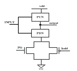
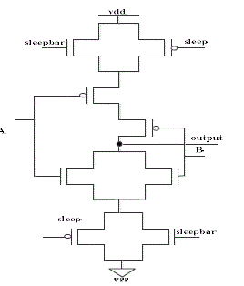
| In sleep transistor technique (gated-VDD and gated-GND) technique, pull-up and/or pull-down or both networks are cut
off from supply voltage or ground using sleep transistors (figure 1). This approach provides very good leakage power
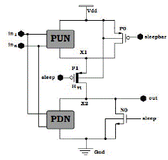
reduction but loses the state information when it enters in to sleep mode. Sleepy Keeper approach introduces additional
keeper transistors to the sleep transistor technique to retain the state of the circuit. As has been concluded in this
reference this circuit methodology has resulted in large dynamic power dissipation. Multiple power gating method of
[10] retains the state but has large associated power consumption. VCLEARIT technique reduces power during sleep
mode but results in to large dynamic power dissipation. [14] Has proposed novel techniques to reduce leakage power in
inverters with ultra low leak operation and state retention. These techniques are applied to combinational logic gates
in this work to achieve better performance. |
NOVEL POWER REDUCTION TECHNIQUES |
| Two novel low leak circuit techniques for logic gates are proposed in this section. |
| • An ultra low leakage power reduction technique with lowest leakage power with lower peak to peak output
voltage swing during active mode of operation. |
| • State retention low leakage technique LPSR with four modes of operation, viz. Active mode , Deep Sleep
mode , State Retention with good 1 and State Retention with good 0. |
A. Ultra Low Leakage Circuit Technique |
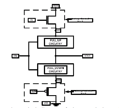
| The generic block diagram of proposed Ultra Low leak technique is provided in figure 5. |
| The Ultra Low leakage logic gate makes use of PMOS transistor as the pull down sleep transistor and NMOS transistor
as the pull up sleep transistor. |
| • Active mode of operation |
| During active mode of operation the sleep signal slp is held at logic 0 value and sleep-bar signal slpb is held at logic
value 1 so that both sleep transistors are on. The node VG is at a higher potential than ground and the node VP is at a
lower potential than VDD. The logic gate thus sees lower potential difference across nodes VP and VG. Thus the
current though the circuit reduces and power dissipation comes down. The gate has correct functionality but higher
logic low and reduced logic high output levels. The power dissipation thus reduces. |
| • Standby mode of operation |
| During sleep or standby mode of operation the sleep signals are complementary of active mode of operation. Now
signal slp is made logic 1 and signal slpb is made logic 0. Sleep Transistors are off, actual power and ground path is
broken, the off resistance increases and leakage current is lowered. The virtual ground and virtual power nodes VG and
VP observe large potentials at their nodes and the potential difference between VP and VG is very less. The current
flowing through the circuit comes down drastically. |
B. Low Power State Retention Technique |
| The generic block diagram of proposed LPSR technique is provided in figure 6. |
| A novel Low Power State Retention (LPSR) circuit technique is proposed in this section. The ultra low leakage gate
can be further improved to provide good logic levels during active mode of operation by using a conventional sleep
transistor both across pull down and pull up paths of logic gate as shown in fig 6. These transistors help us to obtain
good logic levels during active mode of operation. |
| State retention novel low leakage gate has four modes of operation: |
| a. Active mode: both sleep signals are used to switch on the sleep transistors in leakage control block, by making
slp=0 and slpb = 1. The node VG is at ground and the node VP is at VDD. The gate thus sees good potential difference
across nodes VP and VG. The gate functions as per the truth table. |
| b. Deep Sleep mode: both sleep signals are used to switch off the sleep transistors in leakage control block by
making slp=1 and slpb = 0. Thus the actual power and ground path are broken and the gate experiences lower voltage
across the gates; a very high resistance path is established between VDD and ground and the leakage current flowing
through the off transistors reduces significantly and hence least power dissipation is observed. |
| c. State Retention with good 1: The sleep signals are maintained at slp=0 and slpb = 0.The connection to ground
is at VG and full VDD is provided. The state retention takes place during sleep mode. |
| d. State Retention with good 0: The sleep signals are maintained at slp = 1 and slpb = 1.The connection to ground
is complete and virtual VDD is provided. During sleep mode the output state is retained. |
| The states c and d activate one of the sleep control transistors in the pull down path and the pull up path of gate and
hence the state of the gate is preserved if there is no change in input values during standby mode of operation. |
C. Ultra Low Leakage NAND and NOR Gates |
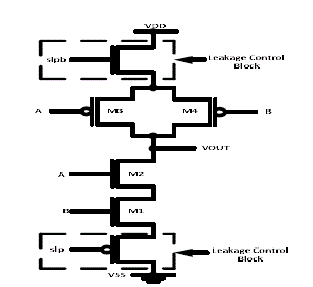
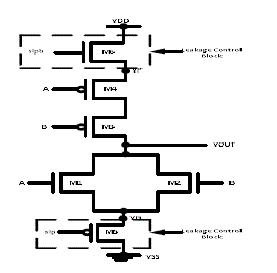
| The Ultra Low leakage gates make use of PMOS transistor as the pull down sleep transistor and NMOS transistor as
the pull up sleep transistor as shown in fig 7 and fig 8. |
| During active mode of operation the sleep signal slp is held at logic 0 value and sleep-bar signal slpb is held at logic
value 1 so that the two sleep transistors M5 and M6 are on. The node VG is at a higher potential than ground and the
node VP is at a lower potential than VDD. The current though the circuit reduces and power dissipation comes down. |
| During sleep or standby mode of operation the sleep signals are complementary of active mode of operation. For the
standby mode of operation the signal slp is made logic 1 and signal slpb is made logic 0. Transistor M5 and M6 are off,
actual power and ground path is broken, the off resistance increases and leakage current is lowered due to stack effect. |
| The ultra low leakage NAND and NOR gates though provides excellent leakage power reduction; the voltage levels at
the output are not at good logic1 and logic 0 values. However this larger reduction in leakage power can be utilised in
situations wherein very long inactive period of operations are normally encountered and reduced logic levels are
acceptable during active mode of operation. |
D. Low Power State Retention NAND and NOR Gates |
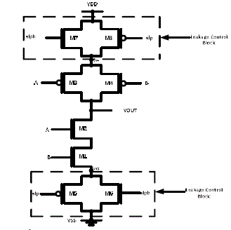
| A low leakage NAND and NOR gates with State Retention are shown in fig 9 and fig 10 respectively. |
| State retention novel low leakage NAND gate has four modes of operation: |
| a. Active mode: both sleep signals are used to switch on the leakage control transistors M5, M6, M7 and M8 by
making slp=0 and slpb = 1. The node VG is at ground and the node VP is at VDD due to the presence of conventional
sleep transistors M5and M6. The NAND gate thus sees good potential difference across nodes VP and VG and
provides good output. |
| b. Deep Sleep mode: both sleep signals are used to switch off the leakage control transistors M5, M6, M7 and
M8 by making slp=1 and slpb = 0. Thus the actual power and ground path are broken and the gate experiences lower
voltage across the gates; a very high resistance path is established between VDD and ground and the leakage current
flowing through the off transistors reduces significantly and hence reduced power dissipation. |
| c. State Retention with good 1: The sleep signals are maintained at slp=0 and slpb = 0, M5 and M8 are ON. The
connection to ground is at VG and full VDD is provided. The state retention takes place with low leakage current due
to off transistors M6 and M7. |
| d. State Retention with good 0: The sleep signals are maintained at slp = 1 and slpb = 1, M6 and M7 are
ON.The connection to ground is complete and virtual VDD is provided. The state retention takes place and leakage
current is lowered due to off transistors M5 and M8.
The states c and d activate one of the sleep control transistors M5 or M6 in the pull down path and M7 or M8 in the pull
up path of gates and hence the state of the gates is preserved if there is no change in input value during standby mode of
operation. |
SIMULATION AND RESULTS |
| All the logic gates discussed in this paper are designed using 90 nm CMOS process technology. The schematic design,
simulation, functionality verification of these gates is performed using cadence virtuoso tool. The static power
dissipation for all input combinations during all operating modes of logic gates and the total power consumption during
pulsed operation are measured using cadence tools. |
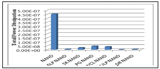
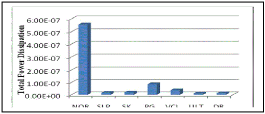
| Table I provides Total power dissipation during pulsed operation for two input NAND and NOR gates. Table II
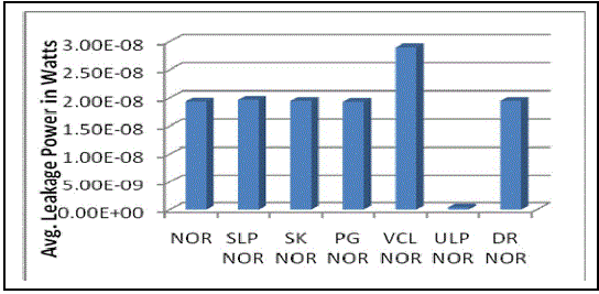
provides comparison of the static power dissipation of all the NAND gates during active mode i.e. when sleep control
signals slp and slpb hold the respective sleep transistors in the ON state and the gates behave in normal manner. This
also provides static power dissipation during standby (sleep) mode of operation. Table III provides the static power
dissipation during active and sleep mode of operation for all the NOR gates. For pulsed operation, transition period is
taken as 2 us duration for all the circuits. All the gates are controlled by the sleep signals of same pulse width and
period for the sake of comparison. Long sleep or inactive period is also introduced to observe the performance during
sleep period. Depending upon whether PMOS or NMOS sleep transistor is driven slp and slpb assume logic states to
make them ON or OFF. The logic values of these sleep signals for different modes of operation in case of different
gates are provided in the tables of observation. |
CONCLUSION |
| The sleep gates using ultra low leak methodology have exhibited lowest leakage current and lowest power. However
during active mode lower output voltage is observed at correct functionality. The sleepy keeper approach though
maintains state during sleep at reduced levels, results in large power dissipation. The proposed LPSR state retention
gates do provide good logic levels at reduced power during active mode of operation. The leakage power during sleep
is also lower and state retention can also be achieved at good logic levels. The Total power dissipation is least. Since
single VTH transistors are used in all the designs to achieve low power the novel techniques provide new choice to the
designers of low power logic gates. |
Tables at a glance |
|
|
Figures at a glance |
 |
 |
 |
 |
| Figure 1 |
Figure 2 |
Figure 3 |
Figure 4 |
 |
 |
 |
 |
| Figure 5 |
Figure 6 |
Figure 7 |
Figure 8 |
 |
 |
 |
 |
| Figure 9 |
Figure 10 |
Figure 11 |
Figure 12 |
 |
 |
 |
 |
| Figure 13 |
Figure 14 |
Figure 15 |
Figure 16 |
|
References |
- Y. Taur, A. Chandrakasan, W. J. Bowhill, and F. Fox, Eds. Piscataway, “CMOS scaling and issues in sub-0.25 μm systems in Design of High- Performance Microprocessor Circuits,” NJ: IEEE, 2001, pp. 27–45.
- Kim N., et al, “Leakage Current: Moore’s Law Meets Static Power,” IEEE COMPUTER, vol. 36, pp. 68–75, December 2003.
- Kaushik Roy, SaibalMukhopadhyay, Hamid Mahmoodi-Meimand ,“Leakage Current Mechanisms and Leakage Reduction Techniques in Deep Submicrometer CMOS Circuits,” Proceedings of the IEEE, vol. 91, No. 2, February 2003.
- Neil Weste, David Harris Ayan Banerjee, CMOS VLSI Design : A Circuits And Systems Perspective , III Edition ,Pearson Education.
- S. Mutoh, T. Douseki, Y. Matsuya, T. Aoki, S. Shigematsu, and J.Yamada, “1-V power supply high-speed digital circuit technology with multithreshold voltage CMOS,” IEEE J. Solid-State Circuits, vol. 30, pp. 847–854, Aug. 1995.
- J.C. Park, V. J. Mooney III and P. Pfeiffenberger, “Sleepy Stack Reduction of Leakage Power,” Proceeding of the International Workshop on Power and Timing Modeling, Optimization and Simulation, pp. 148-158, September 2004.
- AmitAgarwal, Hai Li, and KaushikRoy,“DRG-Cache: A data retention gated-ground cache for low power,”Proceedings of the 39th Design Automation Conference, June 2002.
- M. D. Powell, S. H. Yang, B. Falsafi, K. Roy, and T. N. Vijaykumar. “Gated- VDD: A circuit technique to reduce leakage in cache memories,” Proceedings of the 2000 International Symposium on Low Power Electronics and Design, July 2000.
- S. H. Kim and V. J. Mooney, “Sleepy keeper: a new approach to low leakage power VLSI design,” VLSI-SoC 2006.
- Suhwan Kim, Stephen V. Kosonocky, Daniel R. Knebel, and Kevin Stawiasz ,“Experimental Measurement of A Novel Power Gating Structure with Intermediate Power saving mode”,Proceedings of the 2004 International Symposium on Low Power Electronics and Design (ISLPED).
- Lakshminathan, P. and Nunez,” VCLEARIT: A VLSI CMOS: Circuit Leakage Reduction Technique for Nanoscale Technologies,” Proceedings of the Advanced Low Power Systems Workshop, at the 21st ACM International Conference on Supercomputing (June 2007), pp. 15-22.
- L.Wei, Z. Chen, M. Johnson, K. Roy, Y. Ye, and V. De, “Design and optimization of dual threshold circuits for low voltage low power applications,” IEEE Trans. VLSI Systems, pp. 16–24, Mar. 1999.
- Assaderaghi, D. Sinitsky, S. Parke, J. Bokor, P. K. Ko, and C.Hu, “A dynamic threshold voltage MOSFET (DTMOS) for ultra-low voltage operation,” Dig. Tech. Papers IEEE Int. Electron Devices Meeting, pp. 809–812, 1994.
- Rajani H.P. and Srimannarayana Kulkarni, “Novel Sleep Transistor Techniques for Low Leakage Power in Peripheral Circuits,” unpublished.
|