Magnetic-less multilevel dc–dc converters attract much attention in automotive industry due to their small size, high efficiency, and high temperature operation features. A multilevel modular capacitor-clamped dc–dc converter (MMCCC) is one of the most promising topologies among them with simple control and reduced switch current stress. This paper presents a quasi-resonant technique for multi-level modular switched capacitor dc-dc converter (MMSCC) to achieve zero current switching (ZCS) without increasing cost and Sacrificing reliability. In order to design the converter with the highest efficiency, the analytical power loss equation of an MMCCC should be derived. Also, by considering the stray inductance in the circuit, the optimal design approach should be divided into two cases, over damped case and under damped case. The converter can be designed to achieve high efficiency in both cases by varying circuit parameters. If the circuit is designed in over damped case, huge electrolytic capacitor bank has to be used whereas in under damped cases mall-size multilayer ceramic capacitor can be utilized due to the low capacitance requirement. This ZCS-MMSCC employs the stray inductance distributed in the circuit as the resonant inductor to resonate with the capacitor and provide low dv/dt and di/dt switching transition for the device. The ZCSMMSCC does not utilize any additional components to achieve ZCS, and meanwhile solves the current and voltage spike problem during the switching transition, thus leading to reliable and high efficiency advantages over traditional MMSCC. Furthermore, the ZCS-MMSCC reduces the capacitance needed in the circuit to attain high efficiency. In this case, the bulky capacitor bank with high capacitance in traditional MMSCC to reduce voltage difference and achieve high efficiency is not necessary any more.
Keywords |
| Multilevel Modular Capacitor-Clamped dc–dc converter (MMCCC),zero current switching (ZCS),
stray inductance, analytical power loss equation |
INTRODUCTION |
| In order to obtain the light weight, small size, high efficiency, high power density and integrated dc-dc converter,
switched-capacitor circuits have been investigated since 1970`s. Conventional switched-capacitor dc-dc converters
have some common drawbacks like weak output regulation ability and structurally determinate voltage conversion ratio,
pulsating input current and high current spike, high voltage spike across the switching device, high electromagnetic
interference (EMI), unidirectional power conversion ability. Many approaches have been proposed to achieve voltage
regulation by using duty cycle control. But all this methods have to sacrifice efficiency to achieve the voltage
regulation, which is only acceptable in low power conversion field. Several ZCS techniques by inserting an inductor to
switched-capacitor circuit have been proposed to solve the voltage spike, current spike and EMI problem. However, by
adding a relatively big resonant inductor into the switched-capacitor circuit to achieve ZCS is a contradiction by itself.
Switched-capacitor circuit with a magnetic core is not a switched-capacitor circuit any more, and the good features
such as, high temperature operation, good integration, and small size will be lost. |
| In order to solve theproblemsoftraditionalconverters like high voltage conversion ratio, high current automotive
application A multi-level modular switched-capacitor dc-dc converter (MMSCC) was proposed recently. MMSCC has
modular structure, complementary control scheme, capability of reaching high voltage gain and reduced switch current
stress. It shows good potential in automotive application. Nevertheless, because MMSCC stilluse hard switching, there
still exist several problems limiting its power rating, such as high current spike, high voltage spike, high switching loss and severe EMI noise.With the increasing of power rating or current rating of the MMSCC, the voltage spike and
switching loss problems become more andmore serious. Also, in order to increase the total system efficiency by
reducing voltage difference between capacitors, higher capacitance electrolytic capacitors have to be used. The current
rating of the electrolytic capacitor is small to some extent. In order to meet the high current ripple requirement, a huge
electrolytic capacitor bank has to be used, which will increase the size of the converter significantly. Multi-layer chip
type ceramic (MLCC) capacitor has much better performance than the electrolytic capacitor, such as equivalent series
resistance (ESR), life time, and size in terms of current rating. But the capacitance of MLCC capacitor is very small, so
it is not feasible to use MLCC capacitor for the traditional MMSCC. |
| In this paper presents a quasi-resonant technique for MMSCC that is able to achieve ZCS without increasing cost and
sacrificing reliability. The proposed ZCS strategy employs the distributed stray inductances present in each module of
the circuit resonating with the capacitors to provide zero current turn-on and turn-off to the devices. Because the
MMSCC is especially suitable for high voltage gain with high input current application, the ZCS version also inherits
all the benefits from it. By using the ZCS, the switching loss of the traditional MMSCC is minimized, current spike,
voltage spike and EMI is reduced |
PROPOSED CIRCUIT TOPOLOGY |
| Figure 2.1 shows the proposed four-level ZCS-MMSCC as an example. The circuit works asa four times step-up
converter. |
| By using N-1 modular blocks, a switch and a capacitor, N-level ZCS-MMSCC with n timesvoltage gain can be
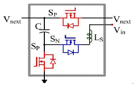
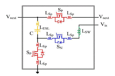
generated. Vinrepresents the ideal input voltage source. LSrepresent theequivalent stray inductance present in each
module of the circuit. SPand SNare the sameswitching devices controlled complementary at 50% duty cycle. C1Xto
C4Xare the capacitorswith the average voltage from one time to four times of input voltage. LSdoes not have to be inthe
position drawn in Figure 2.1, it could be distributed anywhere in series with switches orcapacitors in the circuit. LSis
the sum of the connection wire parasiticinductance LSW, capacitor parasitic inductance LESLand the MOSFETs package
parasiticinductance LSP. Usually the connection wire parasitic inductance LSW is the major part of the stray inductance.
Because all the stray inductance is in series, when the current flows through it |
| Due to the modular structure of the circuit and the stray inductance is distributed equally in each module. The required
stray inductance for resonant is more than 100 times smaller (2nH~13.5 nH) than other ZCS strategies using the same
switching frequency. In case the stray inductance is not sufficiently large or equally distributed in each module, a small
air core could be utilized to promise each module have the same stray inductance for resonant. |
| For traditional MMSCC in high power and high current application, a huge capacitor bank has to be employed in order
to sustain current and increase efficiency, which increases the converter size in a significant manner. The huge
switching loss and voltage spike caused by the large turn-off current is another problem. Considering the stray
inductance present in each module of MMSCC, the capacitance can be designed to resonate with the stray inductance at
switching frequency to provide the zero current switching to the devices. In this case, small size, low ESR, high current
rating and high temperature rating MLCC capacitor with relatively small capacitance can be utilized. The switching
loss of device is minimized, capacitor conduction loss and EMI is also reduced accordingly. Smaller size and higher
efficiency is achieved by using ZCS in MMSCC. Hence, ZCS-MMSCC is more suitable to high power, high current
and high temperature application. |
OPERATION PRINCIPLE |
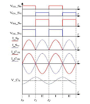
| Figure 3.1 shows the idealized waveform of proposed ZCS-MMSCC under steady-state conditions. The gate signal of
switch SP and SN is complementary, and duty cycle is 50%. Assuming the input voltage is an ideal voltage source. By
considering the stray inductance present in the circuit, when the switch is turned on, the current through the stray
inductance, capacitors and the switch will begin to resonate from zero. By adjusting switching frequency to the
resonant frequency, the current through switch SP, SN and stray inductance will decrease to zero when the switch is
turned off, which is the half period of the sinusoidal waveform. Therefore, the ZCS of the switch is achieved in both
turn on and turn off. The capacitor is charged in half-period with the sinusoidal current waveform and discharged in
another half period also in the sinusoidal shape. So, the current through the capacitor is the sum of the current through
the switch, which is a sinusoidal waveform. When the capacitor is charged, the current is positive; when the capacitor
discharges, the current is negative. The voltage across the capacitor has a dc offset with a sinusoidal ripple. The dc
voltage offset is determined by the capacitor position in the circuit from one time input voltage to n times input voltage.
The voltage ripple is determined by the capacitor current and capacitance. The operation of the circuit can be described
in two states as shown in Figure 3.2 and Figure 3.5 with different switch turned on. |
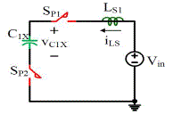
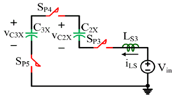
| Figure 3.2 shows the state when SP is turned ON at t = t0 while SN is OFF. During this state C1X is charged by Vin . C3X
is charged by Vin and C2X in series. Figure 3.3 and Figure 3.4 show the two simplified equivalent circuits of state I.
Figure 4.3 shows the situation when Vin ,LS1 , SP1 , C1X and SP2 form a resonant loop. Because of the presence of the
equivalent stray inductance LS , before the switch is turned ON, the current through LS already decreases to zero. The
current through SP will increase from zero when the switch is turned ON, so SP is turned ON at zero current. For the
case shown in Figure 3.3, after LS1 and C1X resonate for half cycle, the current through SP1 and SP2 falls to zero.
Therefore SP1 and SP2 should be turned OFF at this point, so that the switches are turned ON at zero current. In this case
there is only one capacitor in the equivalent circuit other than two capacitors in series in other equivalent circuits. |
| Figure 3.4 shows the situation when Vin , LS3 ,SP3 , C2X ,SP4 , C3X and SP5 form a resonant loop. For this case after LS3
resonate with C2X and C3X in series for half cycle, the current through SP3 , SP4 and SP5 will decrease to zero too. So,
zero current turn off is also realized on these switches. |
| The required stray inductance value is two times smaller than the other circuits assuming the capacitance are the same.
This will not be a problem in the real circuit design and layout; one only need to pay attention to make sure the stray
inductance of all the other loops is twice as large as that of the first resonant loop. |
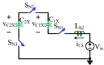
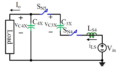
| Figure 3.5 shows the state when SN is turned on at t = t1 while SP is off. During this state, C2X is charged by the Vin and
C1Xin series; C4X is charged by Vin and C3X in series. Figure 3.6 and Figure3.7 show the simplified equivalent circuits
of state II. |
| Figure 3.6 shows the situation when Vin , LS2 , SN1 , C1X , SN2 C2X and SN3 form a resonant loop. Because of the
presence of the LS, the current through SN will also increase its value from zero in a resonant manner. The zero current
turn-on of SN is achieved. For the case shown in Figure 3.6, after LS2, C1X and C2X resonate for half cycle at t = t2, SN1,
SN2 and SN3 will have a zero current turn-off when the current through them decreases to zero. |
| Figure 3.7 shows the situation when VIN, LS4, SN4, C3X, SN5 and C4X form a resonant loop. After LS4 resonate with C3X
and C4X in series for a half cycle, the current through SN3, SN4 and SN5 will also decrease to zero. Hence, zero current
turn off is also realized on these switches. |
SIMULATION RESULTS |
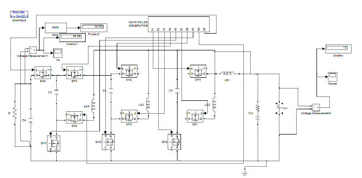
| Figure 4.1 shows the overall simulation model of the proposed topology and is simulated using SIMULINK MATLAB
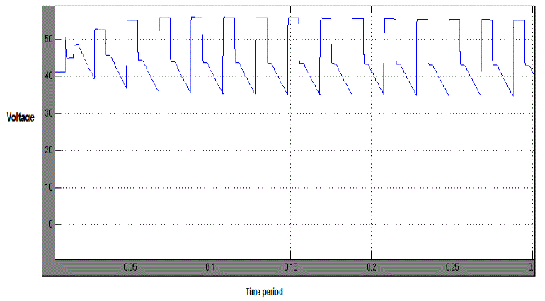
software. Three level of boosting the output is taking place. That is here we are giving an input of 12V and in
simulation we are nearing the value of 38.69V. It is approximately equal to three times of the input. So we can justify
that the simulated prototype model is having three level of boosting the output voltage.The simulation result is
consistent with the theoretical analysis, which verifies the above analysis. |
| Figure 4.2 shows the simulation output with three times boosting of the input voltage |
EXPERIMENT RESULTS |
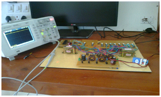
| The hardware set up of the proposed Multi Level Modular Capacitor Clamped DC-DC converter with three level
boosting was done and is shown in Figure 5.1. The hardware model consists of three sections mainly Controller circuit
section, Driver circuit section and the main circuit section. In addition we are using two multi taps transformer with
fivetapping each for providing the gate voltages for the corresponding switches. |
| In this project we are making use of PIC series micro controller 16F877A for producing switching pulses. The micro
controller has got many coding with in it. PIC will execute these coding lines according to the switching pulses, and a
crystal oscillator is introduced. The crystal oscillator can produce pulses at a rate of 20KHz/sec. Thus finally the
switching pulses are produced and it reaches the Driver circuit. The driver circuit has got two main functions to do they
are listed below |
| 1. Amplification of the 5V pulse from the controller to 12V (because, the MOSFET require 12 V DC supply to
function). |
| 2. Isolation (to isolate the main circuit from the controller circuit). So damage to MOSFET is prevented. |
| A. HARDWARE OUTPUT |
CONCLUSION |
| The presented ZCS-MMSCC has all the advantages of ZCS and MMSCC. And it has some special features besides the
features got from ZCS and MMSCC. All the features can be concluded as follows: |
| 1. Reduces dv/dt, di/dt and EMI because of ZCS; |
| 2. Reduces the switching loss which improves efficiency; |
| 3. Uses simple control strategy and possesses modular structure and bidirectional power conversion; |
| 4. Increases the potential power rating by using MLCC capacitor; |
| 5. Reduces the capacitance and capacitor size, which lowers the cost |
| 6. Utilizes distributed stray inductance to achieve ZCS which improves reliability. |
| A new soft-switching operation strategy to the existing MMSCC has been proposed and validated by both simulation
and experiment results. A 40 W, 12 V input three-level converter prototype for automotive application has been built
and tested based on proposed circuit. The ZCS-MMSCC overcomes the current and voltage spike problems of
traditional MMSCC and provides a technically viable soft-switching strategy with circuit layout stray inductance. This
technique could also be applied to the switched-capacitor circuits on a semiconductor chip with very small stray
inductance in the circuit without pushing the switching frequency to megahertz. The proposed ZCS-MMSCC also
shows great potential to high voltage gain and high input current applications. |
Figures at a glance |
 |
 |
 |
 |
 |
| Figure 1 |
Figure 2 |
Figure 3 |
Figure 4 |
Figure 5 |
 |
 |
 |
 |
 |
| Figure 6 |
Figure 7 |
Figure 8 |
Figure 9 |
Figure 10 |
 |
 |
 |
 |
 |
| Figure 11 |
Figure 12 |
Figure 13 |
Figure 14 |
Figure 15 |
|
References |
- R. W. Johnson, J. L. Evans, P. Jacobsen, J. R. Thompson, and M. Christopher, "The changing automotive environment: High temperature electronics" IEEE Trans. Electron. Packag. Manuf., vol.27,no. 3, pp. 164-176, Jul. 2004.
- M. Shen, F. Z. Peng, and L. M. Tolbert, Multilevel DC-DC power conversion system with multiple DC sources, IEEE Trans. Power Electron.,vol. 23, no. 1, pp. 420-426, Jan. 2008.
- T. Funaki, J. C. Balda, J. Junghans, A. S. Kashyap, H. A. Mantooth, F. Barlow,T.Kimoto, and T.Hikihara, Power conversion with SiC devices at extremely high ambient temperatures, IEEE Trans. Power Electron., vol. 22, no. 4, pp. 1321-1329, Jul.2007.
- X. Xu, A. S. Gurav, P. M. Lessner, and C. A. Randall, Robust BME Class-I MLCCs for harsh environment applications, IEEE Trans. Ind.Electron., vol. 58, no. 7, pp.2636-2643, Jul. 2011.
- M.-J. Pan and C. A. Randall, A brief introduction to ceramic capacitors, IEEE Electr. Insulation Mag., vol. 26, no. 3, pp. 44-50, May/Jun. 2010.
- J. F. Dickson, On-chip high-voltage generation in MNOS integrated circuits using an improved voltage multiplier technique,IEEE J. Solid-State Circuits, vol. JSSC-11, no.3, pp. 374 378, Jun. 1976.
- A. IoinoviciSwitched-capacitor power electronics circuits, IEEE Circuits Syst. Mag., vol. 1, no. 3, pp. 37-42, Third Quarter 2001.
- S. V. Cheong, H. Chung, and A. Ioinovici, Inductorless DC-to-DC converter with high power density,IEEE Trans. Ind. Electron., vol. 41, no. 2,pp. 208-215, Apr. 1994.
|