Keywords
|
| CUK Converter, Duty cycle, PI Controller, PWM |
INTRODUCTION
|
| The basic non-isolated Cuk converter shown in Fig.1. It is one of the best basic DC-DC converters because its output voltage is negative and the output voltage may be higher or lower than the input voltage. It is widely used in electrical power system, communication, instruments and meters etc. The advantage of the basic non isolated Cuk converter over the standard buck–boost converter is to provide regulated DC output voltage at higher efficiency and this also reduce ripple currents and reduced switching losses. The basic non isolated Cuk converter is a switching power supply with two inductors, two capacitors, a diode, and a transistor switch. The transfer capacitor Ci stores and transfers energy from the input to the output. |

Fig. 1 Schematic diagram of non-isolated Cuk converter |
OPERATING MODES OF CUK CONVERTER
|
| The converter circuit is divided into two parts as shown in fig.2 and fig.3. During mode 1, when transistor switch is closed then current through inductor Li rises. At the same time the voltage of capacitor Ci reverse biases diode D and turns it off. The capacitor Ci discharges its energy to the circuit formed by Ci, Co, Lo and the load. |

Fig.2 Mode 1: Switch Closed |
| During mode 2, when the input voltage is turned on and switch S is open then diode D is forward biased and capacitor Ci is charged through Li, D and the input supply Vs. The energy which is stored in the inductor Lo is transferred to the load. The diode D and the switch S provide a synchronous switching action. |

Fig.3 Mode 2: Switch Open |
| The Cuk converter can step the voltage either up or down, depending on the duty cycle. The Cuk converter contain the series inductors at both input and output, hence it has much lower current ripple in both circuits. The average output voltage can be calculated in term of the switch duty cycle. |
| D = on time duration of switch/ total switching time period |
 |
| (Where the negative sign indicates voltage inversion) Control schematic of CUK converter output voltage is assumed to be 400V. A simple CUK converter model realize in MATLAB Simulink is shown in fig.5 |

Fig. 4 Simulink model of open loop non- isolated Cuk converter |
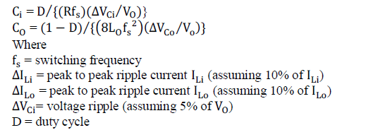
| Design parameter and equations for non-isolated Cuk converter: |
 |
 |
| Calculated value of design variables are D=0.562, Li= 54.47 × 10⁻³ H, L0= 70 × 10-3 H, Ci= 1.125 × 10⁻⁶ F and C0= 0.025 × 10⁻⁶; F |

Fig.5 Open loop response of non-isolated Cuk converter |
| The results of open loop CUK converter is shown in fig.7, which depicts peak to peak ripple voltage (ΔVo) is 54 Volt and maximum o v e r s h o o t of 1 0%. Since the design equations assume constant input voltage and constant load under steady state conditions, the variation of input voltage shall result in fluctuation in output Therefore, a closed loop controller is required with optimized parameters to suit the constant voltage output as per requirement of load. |
CLOSED LOOP CUK CONVERTER
|
| The Simulink Schematic of CUK converter with analog PI controller is shown in fig. 8 |

Fig. 6 Simulink model of closed loop Cuk converter |
| The output voltage is sensed Vout and compared with the input voltage Vref .An error signal is produced which is processed through PI controller to generate a control voltage. The control voltage is used to feed to the PWM generator for control of switch. The PI controller has two parameters namely KP and KI. |
| PI controller has transfer function: C(s) =Kp+(Ki/s) |
| Where,Kp=Proportional gain and Ki= Integral gain |

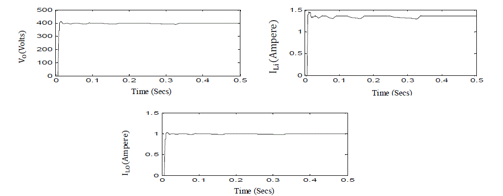
Fig. 7 Closed loop response of Cuk converter |
| The results of closed loop CUK converter is shown in fig.9 which has maximum overshoot of 3.2%, settling time 0.0116 sec and rise time 0.0107 sec. |
| TABLE I AND FIG 8-10 SHOWS VARIATION OF PERFORMANCE PARAMETERS FOR VARIATION OF BOOST INDUCTOR (Li) VALUE IS VARIED. |
 |
 Fig.8 Effect on output voltage (V O) due to variation in boost inductor (Li) Fig.8 Effect on output voltage (V O) due to variation in boost inductor (Li) |
| When the value of boost inductor (Li) increases up to two times of the designed value then output voltage (V0) overshoot, settling time and rise time continuously increases. If the value of boost inductor (Li) decreases from its designed value then output voltage (V0)overshoot increases continuously, settling time remains constant and rise time continuously decreases. |
 Fig.9 Effect on inductor current (ILi) due to variation in boost inductor (Li) Fig.9 Effect on inductor current (ILi) due to variation in boost inductor (Li) |
| When the value of boost inductor (Li) increases up to two times of the designed value then boost inductor current (ILi) overshoot continuously increases, settling time and rise time remains constant. If the value of boost inductor (Li) decreases from its designed value then boost inductor current (ILi) overshoot continuously increases, settling time and rise time remains constant. |
 Fig.10 Effect on inductor current (ILo) due to variation in boost inductor (Li) Fig.10 Effect on inductor current (ILo) due to variation in boost inductor (Li) |
| When the value of boost inductor (Li) increases up to two times of the designed value then filter inductor current (ILi) overshoot, settling time and rise time continuously increases. If the value of boost inductor (Li) decreases from its designed value then filter inductor current ( ILi) overshoot increases continuously, settling time and rise time continuously decreases. |
| TABLE II AND FIG 11-13 SHOWS VARIATION OF PERFORMANCE PARAMETERS FOR VARIATION OF FILTER INDUCTOR (LO) VALUE IS VARIED. |
 |
 |
| Fig.11 Effect on output voltage (VO) due to variation in filter inductor (L0) |
| When the values of ripple filter inductor (L0) increases up to two times of the designed value then output voltage (V0) overshoot decreases, settling time and rise time continuously increases. If the values of ripple filter inductor (LO) decreases up to seven times from its designed value then output voltage (V0) overshoot increases, settling time and rise time continuously decreases. |

Fig.12 Effect on inductor current (ILi) due to variation in filt er inductor (L0) |
| When the value of ripple filter inductor (L0) increases up to two times of the designed value then boost inductor current (ILi) overshoot decreases, settling time and rise time remains constant. If the values of ripple filter inductor (L0) decreases up to seven times from its designed value then boost inductor current (ILi) overshoot increases, settling time and rise time remains constant. |

Fig.13 Effect on inductor current (ILO) due to variation in f ilter inductor (L0) |
| When the value of ripple filter inductor (L0) increases up to two times of the designed value then filter inductor current (ILi) overshoot decreases, settling time and rise time increases. If the values of ripple filter inductor (L0) decreases up to seven times from its designed value then filter inductor current (ILi) overshoot increases, settling time and rise time continuously decreases. |
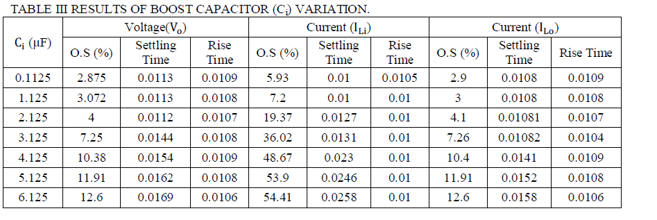
| TABLE III AND FIG 14-16 SHOWS VARIATION OF PERFORMANCE PARAMETERS FOR VARIATION OF BOOST CAPACITOR (Ci) VALUE IS VARIED. |
 |

Fig.14 Effect on output voltage (VO) due to variation in boost capacitor (Ci) |
| When the value of boost capacitor (Ci) increases up to six times of the designed value then output voltage (V0) overshoot and settling time increases and rise time decreases. If the values of boost capacitor (Ci) decreases from the designed value then output voltage (V0) overshoot decreases, settling time remains constant and rise time increases. |

Fig.15 Effect on inductor current (ILi) due to variation in boost capacitor (Ci) |
| When the value of boost capacitor (Ci) increases up to six times of the designed value then boost inductor current (ILi) overshoot and settling time continuously increases and rise time remains constant. If the values of boost capacitor (Ci) decreases from the designed value then boost inductor current (ILi) overshoot decreases, settling time remains constant and rise time increases. |

Fig.16 Effect on inductor current (ILO) due to variation in boost capacitor (Ci) |
| When the value of boost capacitor (Ci) increases up to six times of the designed value then filter inductor current (ILi) overshoot and settling time continuously increases and rise time decreases. If the values of boost capacitor (Ci) decreases from the designed value then filter inductor current (ILi) overshoot decreases, settling time remains constant and rise time increases. |
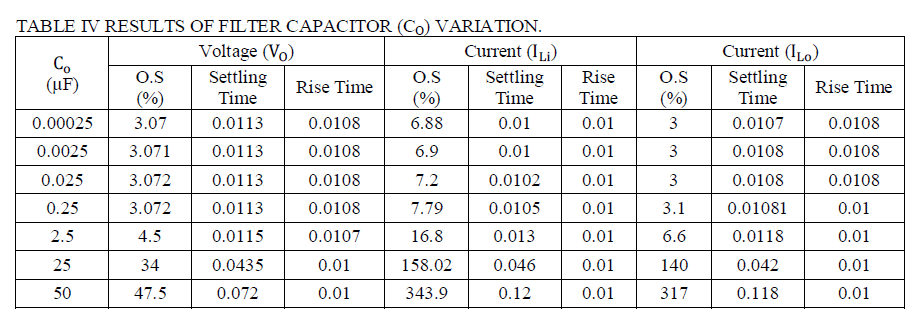
| TABLE IV AND FIG 17-19 SHOWS VARIATION OF PERFORMANCE PARAMETERS FOR VARIATION OF FILTER CAPACITOR (CO) VALUE IS VARIED. |
 |
 |
| When the value of filter capacitor (C0) increases up to two thousand times of the designed value then output voltage (V0) overshoot and settling time continuously increases however rise time decreases and finally attain a constant value. If the values of filter capacitor (C0) decreases up to hundred times from the designed value then output voltage (V0) overshoot decreases, settling time and rise time remains constant. |
 |
| When the value of filter capacitor (C0) increases up to two thousand times of the designed value then boost inductor current (ILi) overshoot and settling time continuously increases however rise time remains constant value. If the values of filter capacitor (C0) decreases up to hundred times from the designed value then boost inductor current (ILi) overshoot decreases, settling time and rise time remains constant. |
 |
| When the value of filter capacitor (C0) increases up to two thousand times of the designed value then output filter inductor current (ILi), settling time continuously increases however rise time decreases and finally attain a constant value. If the values of filter capacitor (C0) decreases up to hundred times from the designed value then filter inductor current (ILi) overshoot become constant, settling time slowly decreasing and rise time increased. |
CONCLUSION
|
| The parametric variation analysis of non-isolated CUK converters has been carried out for constant voltage applications considering inductor and capacitor as performance parameters. Non-isolated CUK converter has been designed to deliver 400 volts DC to a 400 watt load. Performance and applicability of this converter is presented on the basis of simulation in MATLAB SIMULINK. The design concepts are validated through simulation and results obtained show that a closed loop system using buck-boost converter will be highly stable with high efficiency. Cuk converter can be used for universal input voltage and wide output power range. The Cuk converter uses capacitive energy transfer. In the Cuk converter overshoot and settling time varies much if there is small change in boost capacitor. The closed loop Cuk converter has an efficiency of 98.69%. |
Tables at a glance
|
References
|
- Sanjeev Singh and Bhim Singh, “A Voltage-Controlled PFC Cuk Converter-Based PMBLDCM Drive for Air-Conditioners,” in Proc. IEEETRANS. ON INDUSTRY APPLICATIONS, VOL. 48, NO. 2, Apr. 2012, pp. 832-838.
- Sanjeev Singh and Bhim Singh, “Power quality improved PMBLDCM drive for adjustable speed application with reduced sensor buck-boost PFCconverter” in proc. IEEE 11th ICETET, 2011, pp.180-184.
- Sanjeev Singh and Bhim Singh, “Comprehensive study of single-phase AC-DC power factor corrected converters with high-frequency isolation”IEEE Trans. on Industrial Informatics, vol. 7, no. 4, Nov. 2011, , pp. 540-556.
- Boopathy.K and Dr.Bhoopathy Bagan .K, “Buck Boost converter with improved transient response for low power applications” in Proc. IEEE SIEA, Sep 2011, pp. 155-160.
- Altamir Ronsani and Ivo Barbi, “Three-phase single stage AC-DC buck-boost converter operating in buck and boost modes” in Proc. IEEE, 2011, pp.176-182.
- Sanjeev Singh and Bhim Singh, “An adjustable speed PMBLDCM drive for air conditioner using PFC Zeta converter,” Int. J. Power Electron. (IJPElec), vol. 3, no. 2, pp. 171–188, Apr. 2011.
- Sanjeev Singh and Bhim Singh, “Power Electronics, Drives and Energy Systems (PEDES),” in Proc. IEEE PEDES’2010.
- Sanjeev Singh and Bhim Singh, “Single-phase power factor controller topologies for permanent magnet brushless DC motor drives,” in IET Power Electron., 2010, Vol. 3, Iss. 2, pp. 147–175. Qq
- Sanjeev Singh and Bhim Singh, “A voltage controlled adjustable speed PMBLDCM drive using a single-stage PFC half-bridge converter,” in Proc. IEEE APEC’10, 2010, pp. 1976–1983.
- Marcos Orellana, Stephane Petibon and Bruno Estibals, “Four switch buck-boost converter for photovoltaic DC-DC ower applications” in proc. IEEE, ISGE, 2010, pp.469-474.
- B. Singh, B. N. Singh, A. Chandra, K. Al-Haddad, A. Pandey, and D. P. Kothari, “A review of single-phase improved power quality ac–dc converters,” IEEE Trans. Ind. Electron., vol. 50, no. 5, pp. 962–981, Oct. 2003.
- S. M. ÃâÃâ uk, “Modeling, Analysis, and Design of Switching Converters,” Ph.D. dissertation, California Institute of Technology, Pasadena, Nov. 1976.
|