Network-On-Chip (NOC) structure makes a fitting substitution for system on chip designs incorporating large number of processing cores. In network the main source of power dissipation is in the network on chip links. The dynamic power dissipation in links is major contributor to the power consumption in NOC. This effort investigsates the reduction of transition activity using gray coding schemes. Our advanced scheme does not require any change of the routers and link architecture. The future scheme uses the binary to gray conversion at the transmitter and gray to binary conversion at the receiver. An investigational result has shown the effectiveness of the proposed schemes, with respect of power dissipation and area overhead in the Network Interface (NI) as compared with data encoding.
Keywords |
| Binary to gray conversion, Data encoding, Interconnection on chip, Low power, Network-on-chip
(NOC), Power analysis, Gray to binary conversion. |
INTRODUCTION |
| In accordance with Moore‘s law density of transistors doubles every 18 months and currently we all know that
there are millions of FETs on a single chip is known as VLSI. Integrating these FETs combine together to perform set
of operations and applications such as DSP, Communications, Robotics and medical filed. Network on chip is a
communication subsystem an on integrated circuit typical between IP cores in a system on a chip (SOC). NOC
Technology applied methods to on chip communication and brings notable improvement over conventional bus and
crossbar interconnections. NOC improves the scalability of SOC‘s and the power efficiency of complex SOC‘s
compared to other designs. A network on chip uses packets to transfer data between IP core interfaces within a chip.
The NOC based system on chips imposes various design issues on the fabrication of such integrated chips. Firstly, the
suitable topology for the target NOCs such that the presentation supplies and design constraints are satisfied. Secondly,
the design of network interfaces to access the on chip network and routers provide the physical interconnection
mechanisms to transport data between processing cores. Finally, as technology scales and switching speed increases,
future network on chips will become more responsive and prone to errors and faults. |
| On-chip communication problems are more relevant to compare to the computational relevant problems. The
computational subsystem has major objectives like including cost, performance, power dissipation, energy
consumption, reliability thus, the total power of a system on chip depends on the communication subsystem. |
| In this work, we are going to reducing the power dissipation in the network links. The power dissipation in the
network on chip is relevant to the power dissipation in the routers and Network Interfaces(NIs). For highly integrated
electronic systems, the reduction of on-chip power dissipation is a essential one. The amount of power consumption in
a NOC grows linearly by increasing the amount of bit transitions in consequent data packets sent through the
interconnect architecture. By using the coding schemes we are reducing the switching activity on both wires and logic
in this way we are reducing the power consumption in the NOC. The power due to self-switching activity of individual
bus lines while ignoring the power dissipation owing to their coupling switching activity [2]. Data encoding is mainly
used for reducing the number of bit transition over interconnects. Bus invert (BI), Adaptive coding, Gray coding and Transition method these are the various encoding techniques used in the NOC. We are using the data encoding with
gray input is mainly reducing the power dissipation on the NOC. |
| This paper is organized as follows. We briefly discuss Previous Work in Section II, while Section III discuss
an overview of the proposed encoding technique. The advanced data encoding schemes along with possible hardware
implementations and their analysis are described in Section IV. The results for the hardware overhead, power and
energy savings and performance of the proposed encoding schemes these are discuss in Section V. |
RELATED WORK AND MOTIVATION |
| The accessibility of chips are growing every years. In the next several years, the availability of cores with
1000 cores is foreseen[3]. Since the focus of this paper is on reducing the power dissipated by the links, here we briefly
review some of the works in the area and link power reduction. Also these include some technique. There are, use of
shielding [4], [5], increasing line-to-line spacing [6], [7], and repeater insertion [8]. Thus the above all the techniques
having large area overhead. Another one method is the data encoding technique it mainly focus on reducing the link
power reduction. The data encoding technique is classified into two categories. In the first category is mainly
concentrate on minimizing the power due to self-switching activity of each bus lines and avoid the power dissipation
due to coupling switching activity. In this category, bus invert [BI] [9] and INC-XOR [10] have been proposed. When
the random patterns are transmitted via these lines. On the other hand, gray code [11], T0 [12], working-zone encoding
[13], and T0-XOR [14] have been proposed for the case of correlated data patterns. |
| In this first category of encoding is not suitable for applied in deep sub-micron meter technology nodes where
the coupling capacitance is a main part of the total interconnects capacitance. This causes the power due to the coupling
switching activity to become a large portion of the link power reduction. In the second category concentrate on
reducing power dissipated through the reduction of the coupling switching [7], [14]-[15]. The technique proposed in
[16], proposed a method on power effective Bus Invert. In [15] they presented a method based on Odd/Even Bus-Invert
techniques. If the number of switching transitions is half of the line width means the odd inversion is performed. In [9],
the number of transitions from 0 to 1 for two data packets is counted. The number of 1‘s in the data packet is larger
than the half of the links means the inversion will be performed and the number of 1‘s is reduced to 0 transitions when
the packets are transfer through the links. In [17], the technique is used to reducing the coupling switching. From this
method, the encoder counts the Type I transitions with the weighting coefficient of one and the Type II transitions with
the weighting coefficient of two. If the number of 1‘s is larger than half of the links means the inversion will be
performed and it reducing the power consumption on the links. The technique proposed in [1] using the data encoding
technique. This technique illustrate if the bits are encoded before they are injected into the network with the goal of
minimizing the self-switching and the coupling switching in the links. These two are the main reason for the link power
dissipation. Here they are classified the encoding technique into three scheme based on the four Types. In scheme 1
using the odd inversion and scheme 2 using the both odd inversion and full inversion and scheme 3 using the both odd,
full and even inversion. Based on the odd, full and even inversion the power dissipation is reduced on the Network on
chip (NOC) links. In this paper we present gray encoding technique, which focused on reducing the errors during the
transition from transmitter to receiver and reducing the power dissipation in the links. |
OVERVIEW OF THE PROPOSAL |
| The basic idea of the proposed technique is the packets are transferred through the network after that the bits
are encoded. This technique is more helping to reduce the switching activity and coupling switching activity in the
links traversed by the packets. This self-switching activity and coupling switching activity are responsible for the link
power dissipation. Here we refer to end-to-end scheme. Based on the end to end scheme we are having a better
advantage. The advantage is a pipeline nature of the wormhole switching technique [18]. Since the same sequence of
all the packets passes through all the links of the routing path. The NI may provide the same power saving for all the
links. The advanced scheme, an encoder and decoder block are added to the NI. The gray input is applied for all the
three scheme encoders. The gray coding technique is used for the error correction application. The encoder encodes all the leaving bits of the packets other than header bit such that the power dissipated by the inter router and point-to—
point link is minimized [19]. |
PROBOSED ENCODING SCHEMES |
| The main goal of the proposed encoding scheme is to reduce the power dissipation by minimizing the coupling
transition activities on the links of the interconnection network. In [17], they are classified four types of coupling
transitions. A Type I occurs when one of the line is switches and remaining one is unchanged. A Type II occurs when
one of the lines switches from low to high and another one is switches from high to low. A Type III occurs both the
lines switches simultaneously. A Type IV occurs when both the lines are remains unchanged. The coupling switching
activity (Tc) is defined as a weighted sum of different types of coupling transition contribution [17]. Therefore |
| Tc = K1T1 + K2T2 + K3T3 + K4T4 eq. (1) |
| Where Ti is the average number of Type I transition and Ki is the corresponding weight |
| A. Gray code: |
| The gray code is also knows as reflected binary code. It is a binary numeral system, where two successive
values differ in only one bit. The reflected binary code was originally designed to prevent false output from
electromagnetic switches. It is mainly used for error correction application in digital communications. |
| B. Problem with binary code: |
| The problem with binary codes is that, with real switches. The switches will change states exactly in
synchronously. In binary code, the two successive values differ in one or more bits. if the output pass through a
sequential system then the sequential system may store a false value. The gray code solves the above problem by
changing only one bit at a time. |
| C. Scheme I: |
| In scheme 1, our main goal is to reducing the number of Type 1 transitions and Type 2 transitions. Type 1
transitions is converted into Type III and Type IV transitions and Type II transitions is converted into Type I
transitions. This scheme compares the two data‘s based on to reducing the link power reduction by doing odd
inversion or no inversion operation. |
| Ty > Tx (2) |
| Ty > 0.5 (w-1) eq. (3) |
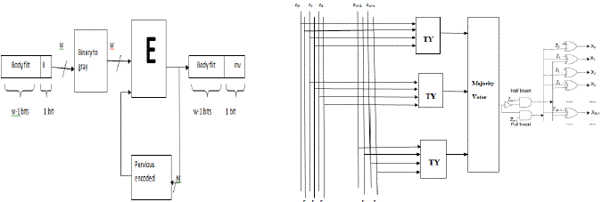
| The general block diagram in Fig. 1(a) is same for scheme 1, scheme 2 and scheme 3. The w-1 bit is given to
the one input of the binary to gray conversion block. This block converts the original binary input into gray output. The
output of the gray code is given as input of encoder block and another input of the encoder block is the previously
encoded output. The encoder block compares these two inputs and performing the any one of the inversion based on the
transition types. The block E is vary for all the three schemes. Comparing the current data and previous encoded data to
decide which inversion is performed for link power reduction. Here the TY block this takes two adjacent bits from the
given inputs. From these two input bits the TY block checks what type of transitions occurs, whether more number of
type 1 and type 2 transitions is occurring means it set the output state to 1, otherwise it set the output to 0. The odd
inversion is performed for these type of transitions.Then the next block is the Majority code it checks the state, if the
number of one‘s is greater than zeros or not and it implemented using a simple circuit. The last stage using the XOR
circuits, these circuit is used to perform the inversion on odd bits. The decoding is performed by simply inverts the
encoder circuit when the inverting bit is high. |
| D. Scheme II: |
| In scheme II, our main goal is to reducing the number of Type II transitions. Type II transitions are converted
into Type IV transitions. This scheme compares the two data‘s based on to reducing the link power reduction by doing
full inversion or odd inversion or no inversion operation. |
| T2 > T4
** eq. (4) |
| Full and odd inversion based this advanced encoding architecture consist of w-1 link width and one bit for
inversion bit which indicate if the bit travel through the link is inverted or not. W bits link width is considered when
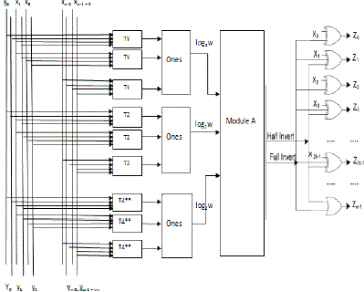
there is no encoding is applied for the input bits. Here the TY block from scheme 1 is added in scheme 2. This takes
two adjacent bits from the given inputs. From these two input bits the TY block checks what type of transitions occurs.
We have T2 and T4
** blocks which determines if any of the transition types T2 and T4
**occur based on the link power
reduction. The number of ones blocks in the next stage. The output of the TY, T2 and T4
** send through the number of
one‘s blocks. The output of the ones block is log 2 w. The first ones block is used to determine the number of transitions
based on odd inversion. The second ones block determines the number of transitions based on the full inversion and the
then another one ones block is used to determine the number of transitions based on the full inversion. These inversions
are performed based on the link power reduction. Based on these ones block the Module A takes the decision of which
inversion should be performed for the link power reduction. For this module is satisfied means the output is set to ‗1‘.
None of the output is set to ‗1‘ if there is no inversion is takes place. The module A is implemented using full adder and
comparator circuit. |
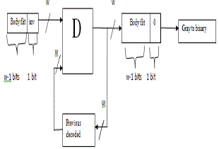
| The block diagram of the decoder is shown in Fig.3. The w-1 bits input is applied in the decoder circuit and
another input of the decoder is previous decoded output. The decoder block compares the two input data‘s and
inversion operation is performed and w-1 bits output is produced. The remaining one bit is used to indicate the
inversion is performed or not. Then the decoder output is given to the gray to binary block. This block converts the
gray code into original binary input. |
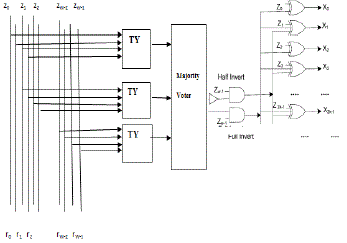
| In decoder circuit diagram (Fig.4.) consist of TY block and Majority vector and Xor circuits. Based on the
encoder action the TY block is determined the transitions. Based on the transitions types the majority blocks checks the
validity of the inequality given by(2). The output of the majority voter is given to the Xor circuit. Half inversion, full
inversion and no inversion is performed based on the logic gates. |
| E. Scheme III: |
| In scheme III, we are adding the even inversion into scheme II. Because the odd inversion converts Type I
transitions into Type II transitions. From table II, T1
**/T1
*** are converted into Type IV/Type III transitions by the flits
is even inverted. The link power reduction in even inversion is larger than the Odd inversion. |
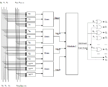
| The encoding architecture (Fig.5) in scheme III is same of encoder architecture in scheme I and II . Here we
adding the Te block to the scheme II. This is based on even invert condition, Full invert condition and Odd invert
condition. It consist of w-1 link width input and the w bit is used for the inversion bit. The full, half and even Inversion
is performed means the inversion bit is set ‗1‘, otherwise it set as ‗0‘.The TY, Te and T4** block determines the
transition types T2, Te and T4**. The transition types are send to the number of ones block. The Te block is determined
if any of the detected transition of types T2, T1** and T1**. The ones block determines the number of ones in the
corresponding transmissions of TY, T2, Te and T4**. These number of ones is given to the Module C block. This block
check if odd, even, full or no invert action corresponding to the outputs ‗10‘, ‗01‘, ‗11‘ or ‗00‘ respectively, should be
performed. The decoder architecture of scheme II and scheme III are same. |
RESULTS AND DISCUSSION |
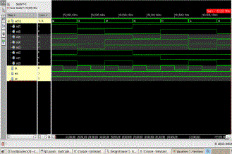
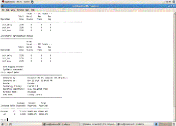
| Fig.6. shows the simulation result of scheme I (reducing Type I and Type II transitions) using gray encoding
technique. The output of the scheme I reducing the number of Type I and Type II transitions by using the odd invert
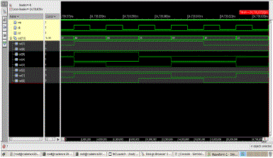
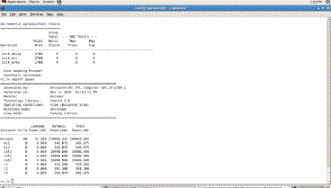
condition. Fig.7. shows the simulation result of scheme II (convert Type II transitions into Type IV ) using gray
encoding techniques. In scheme II the number of type II transition is converted into Type IV transitions by using the
odd and full inversion condition. |
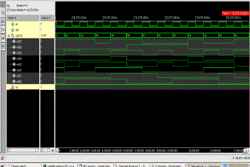
| Fig.8. shows the simulation result of scheme III (Type I (T1
***) converted into Type II) using the gray
encoding. The output of the scheme III reducing the number of Type I (T1
***) into Type II transitions by using odd, full
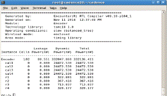
and even inversion. Fig.9. shows power calculation of scheme I (reducing Type I and Type II transitions) using gray
encoding technique. And the leakage power is reduced to 42% compared to data encoding [1]. |
| Fig.10. shows the power calculation for scheme II (convert Type II transitions into Type IV) using gray
encoding techniques. And the leakage power is reduced to 42% compared to data encoding technique [1]. Fig.11.
shows the power calculation for scheme III (convert Type I (T1
***) into Type II transitions) using gray encoding
techniques. And the leakage power is reduced to 42% compared to data encoding technique[1]. |
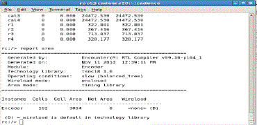
| Fig.12.shows area calculation of gray encoding technique. Area is reduced to less than 5% compared to data
encoding [1]. |
CONCLUSION AND FUTURE WORK |
| In this work, the gray encoding technique is implemented for reducing the transition activity in the NOC. This
gray encoding scheme aimed at reducing the power dissipated by the links of an NOC. In fact links are responsible for
a significant fraction of the overall power dissipated by the communication system. The proposed encoding schemes
are agnostic with respect to the underlying NOC architecture in the sense that our application does not require any
modification neither in the links nor in the links. The proposed architecture is coded using VERILOG language and is
simulated and synthesized using cadence software. Overall, the application scheme allows savings up to 42% of power
dissipation and with less than 5% area overhead in the NI compared to the data encoding scheme. |
| In the future, the Network On Chip (NOC) implementation using different types of router technique will be
analyzed . Comparison on many encoding techniques such as gray encoding techniques will be analyzed in which the
area, delay, power and the performance of the NOC will be investigated and use for high speed applications. |
Tables at a glance |
 |
 |
| Table 1 |
Table 2 |
|
Figures at a glance |
 |
 |
 |
 |
| Figure 1 |
Figure 2 |
Figure 3 |
Figure 4 |
 |
 |
 |
 |
| Figure 5 |
Figure 6 |
Figure 7 |
Figure 8 |
 |
 |
 |
 |
| Figure 9 |
Figure 10 |
Figure 11 |
Figure 12 |
|
References |
- Nima Jafarzadeh, Maurizio Palesi, Ahmad , and Afzali-Kusha, ―Data Encoding Techniques for Reducing Energy Consumption in Network-on-Chip‖ IEEE Trans. Very Large ScaleIntegr. (VLSI) Syst,Mar.2014.
- International Technology Roadmap for Semiconductors. (2011) [Online].Available: http://www.itrs.net
- D. Yeh, L. S. Peh, S. Borkar, J. Darringer, A. Agarwal, andW. M. Hwu, ―Thousand-core chips roundtable,‖ IEEE Design Test Comput., vol. 25, no. 3, pp. 272–278, May–Jun. 2008.
- D. Yeh, L. S. Peh, S. Borkar, J. Darringer, A. Agarwal, andW. M. Hwu, ―Thousand-core chips roundtable,‖ IEEE Design Test Comput., vol. 25, no. 3, pp. 272–278, May–Jun. 2008.
- M. Ghoneima, Y. I. Ismail, M. M. Khellah, J. W. Tschanz, and V. De, ―Formal derivation of optimal active shielding for low-power on-chip buses,‖ IEEE Trans.Comput.-Aided Design Integr. Circuits Syst., vol. 25, no. 5, pp. 821–836, May 2006.
- L. Macchiarulo, E. Macii, and M. Poncino, ―Wire placement for crosstalk energy minimization in address buses,‖ in Proc. Design Autom.Test Eur. Conf. Exhibit., Mar. 2002, pp. 158–162.
- R. Ayoub and A. Orailoglu, ―A unified transformational approach for reductions in fault vulnerability, power, and crosstalk noise and delay on processor buses,‖ in Proc. Design Autom. Conf. Asia South Pacific, vol. 2. Jan. 2005, pp. 729–734.
- K. Banerjee and A. Mehrotra, ―A power-optimal repeater insertion methodology for global interconnects in nanometer designs,‖ IEEETrans. Electron Devices, vol. 49, no. 11, pp. 2001–2007, Nov. 2002.
- M. R. Stan and W. P. Burleson, ―Bus-invert coding for low-power I/O,‖ IEEE Trans. Very Large Scale Integr. (VLSI) Syst., vol. 3, no. 1, pp. 49–58, Mar. 1995.
- S. Ramprasad, N. R. Shanbhag, and I. N. Hajj, ―A coding framework for low-power address and data busses,‖ IEEE Trans. Very Large ScaleIntegr. (VLSI) Syst., vol. 7, no. 2, pp. 212–221, Jun. 1999.
- C. L. Su, C. Y. Tsui, and A. M. Despain, ―Saving power in the control path of embedded processors,‖ IEEE Design Test Comput., vol. 11, no. 4, pp. 24–31, Oct.– Dec. 1994.
- L. Benini, G. De Micheli, E. Macii, D. Sciuto, and C. Silvano, ―Asymptotic zero-transition activity encoding for address busses in low-power microprocessor-based systems,‖ in Proc. 7th Great Lakes Symp. VLSI, Mar. 1997, pp. 77–82.
- E. Musoll, T. Lang, and J. Cortadella, ―Working-zone encoding for reducing the energy in microprocessor address buses,‖ IEEE Trans. VeryLarge Scale Integr.(VLSI) Syst., vol. 6, no. 4, pp. 568–572, Dec. 1998.
- S. Youngsoo, C. Soo-Ik, and C. Kiyoung, ―Partial bus-invert coding for power optimization of application-specific systems,‖ IEEE Trans. VeryLarge Scale Integr. (VLSI) Syst., vol. 9, no. 2, pp. 377–383, Apr. 2001.
- Z. Yan, J. Lach, K. Skadron, and M. R. Stan, ―Odd/even bus invert with two-phase transfer for buses with ,‖ in Proc. Int. Symp. LowPower Electron. Design, 2002, pp. 80–83.
- Z. Yan, J. Lach, K. Skadron, and M. R. Stan, ―Odd/even bus invert with two-phase transfer for buses with ,‖ in Proc. Int. Symp. LowPower Electron. Design, 2002, pp. 80–83.
- K. W. Ki, B. Kwang Hyun, N. Shanbhag, C. L. Liu, and K. M.Sung, ―Coupling-driven signal encoding scheme for low-power interface design,‖ in Proc.IEEE/ACM Int. Conf. Comput.-Aided Design, Nov. 2000, pp. 318–321.
- M. Palesi, G. Ascia, F. Fazzino, and V. Catania, ―Data encoding schemes in networks on chip,‖ IEEE Trans. Comput.-Aided Design Integr. CircuitsSyst., vol. 30, no. 5, pp. 774–786, May 2011.
- M. Palesi, G. Ascia, F. Fazzino, and V. Catania, ―Data encoding schemes in networks on chip,‖ IEEE Trans. Comput.-Aided Design Integr. CircuitsSyst., vol. 30, no. 5, pp. 774–786, May 2011.
|