Keywords
|
| Space vector Pulse width Modulation (SVPWM), Three Phase Inverter, Total Harmonic Distortion (THD), Switching Stress. |
I. INTRODUCTION
|
| Three phase voltage source inverters are widely used in variable speed AC motor drive applications since they provide variable voltage and variable frequency output through pulse width modulation control [1] [2]. The most widely used PWM method is the carrier-based sine-triangle PWM method due to simple implementation in both analog and digital realization [2] [3]. However in this method the DC bus utilization is low (0.5Vdc). This has led to the investigation into other techniques with an objective of improving in the DC bus utilization [1] [3]. The PWM technique termed as Space Vector PWM based on space vector theory was proposed by de Broeck et.al (1988) and Ogasawara et.al (1989) which offers superior performance compared to the carrier –based sine-triangle PWM technique I terms of higher DC bus utilization and better harmonics performance [3]. Further, this technique offers easier digital realization. The research in PWM schemes has intensified in the last few decades. The main aim of any modulation technique is to obtain a variable output with a maximum fundamental component and minimum harmonics [3] [4]. |
| The problem of underutilization of the DC bus voltage led to the development of the Third order harmonic-injection PWM (THIPWM) and Space Vector PWM (SVPWM) [5] [6]. In 1975, Buja developed this improved sinusoidal PWM technique which added a third –order harmonic content in the sinusoidal reference signal leading to a 15.5% increase in the utilization rate of the DC bus voltage. In 1988, Van Der Broeck developed the SVPWM technique which has also increased the utilization of DC bus voltage by 15.5%. Here these two techniques have similar results, but their methods of implementation are completely different [7] [8]. With the development of microprocessors SVPWM has become one of the most important PWM methods for three phase inverter [9] [10] [11]. The maximum peak fundamental magnitude of the SVPWM technique is about 90.6% increase in the maximum voltage compared with conventional sinusoidal modulation [12] [17]. |
| In this paper having some detailed discussion about 2-level SVPWM based three phase voltage source inverter fed induction motor. In all the research papers discussed the performance analysis of three phase voltage source inverter fed induction motor by only one possible switching sequence in 2-level SVPWM. But there are four possible switching sequences are there in 2-level SVPWM. This paper tries to focus on the performance characteristics of three phase voltage source inverter fed induction motor in all four possible switching sequences. The MATLAB/SIMULINK is used to analyze its performance and compared its results. The result parameters are DC bus utilization, efficiency of the inverter, load voltage and load currents. |
| The paper organized in ten sections. Section II gives small introduction recording SVPWM principles. Section III introduces various steps involved in the switching time calculations. Section IV introduces the first possible switching sequence and its switching time calculation and its output waveforms. Section V introduces the second possible switching sequence and its switching time calculation and its output waveforms. Section VI introduces the third possible switching sequence and its switching time calculation and its output waveforms. Section VII introduces the fourth possible switching sequence and its switching time calculation and its output waveforms. Section VIII shows the comparative results of all the four possible switching sequences. Section IX shows the extension of the proposed scheme to the Z- source and T- source inverters. Section X concludes the paper. |
II. SVPWM PRINCIPLE’S
|
| Space Vector Modulation (SVM) was originally developed as a vector approach to pulse width modulation (PWM) for three phase inverter. It is a more sophisticated technique for generating sine wave that provides a higher voltage to the motor with lower harmonic distortion [13]. The main aim of any modulation technique is to obtain variable output having a maximum fundamental component with minimum harmonics. SVPWM method is an advance: computation intensive PWM method and possibly the best techniques for variable frequency drive applications. |
| The principle of pulse width modulation is explained by using the figure-1[18]. The figure-1 (a) shows a circuit model of a single phase inverter with a center-tapped grounded DC bus. The figure-1 (b) illustrates principles of pulse width modulation. |
 |
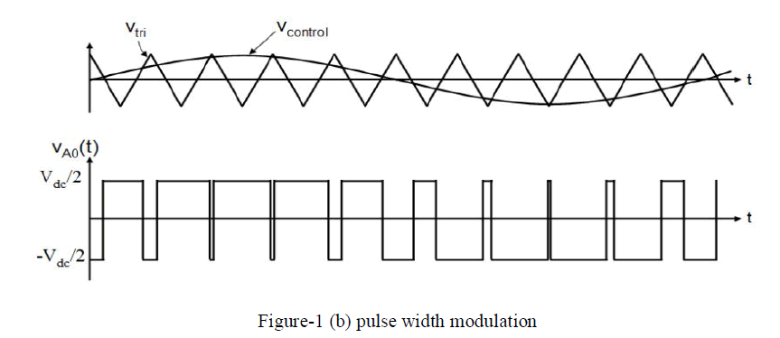 |
| From the figure-1 (b), the inverter output voltage is determined by the following ways. |
| 1. When V control > V triangle means VAO = VDC/2 |
| 2. When V control < V triangle means VAO = -VDC/2 |
| Also the inverter output voltage has the following features. |
| 1. PWM frequency as same as the V triangle frequency. |
| 2. Amplitude is controlled by the peak value of V triangle. |
| 3. The fundamental frequency is controlled by the frequency of V control. |
| 4. Modulation index (M) is defined as |
| M=Vcontrol/Vtriangle;0 ≤ M ≤ 1 |
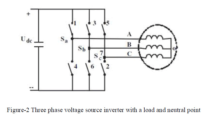
| The circuit model of a typical three phase voltage source inverter is shown in figure-2. S1 to S6 are the sin's power switches that shape the output, which are controlled by the switching variables a, a’, b, b’, c, and c’. When an upper switch (a, b, c) are switched ON ie) a, b and c = 1, the corresponding lower switches (a’, b’, c’) switched OFF myself ie) a’, b’ and c’ = 0. The upper switches and lower switches are complimentary to each other. Therefore the ON and OFF states of the upper and lower switches determines the output voltages [18]. The SVPWM is a different approach from PWM modulation based on space vector representation of the voltage in the α-β plane. |
 |
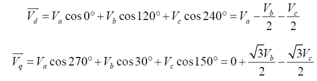
| The space vector concept, which is derived from the rotating field of the induction motor, is used to modulate the inverter output voltage. In the modulation technique the three phase quantities can be transformed into their equivalent two-phase quantity either in synchronously rotating frames or stationary frame. From these two-phase components, the reference vector magnitude can be found and used for modulating the inverter output [6] [13] [16] [19]. The process of obtaining the rotating space vector is explained in the following section. Considering the stationary reference frame, let the three phase sinusoidal voltage component be |
| Va = Vmsinwt |
| Vb = Vmsin(wt-2π/3) |
| Vc = Vmsin(wt-4π/3) (1) |
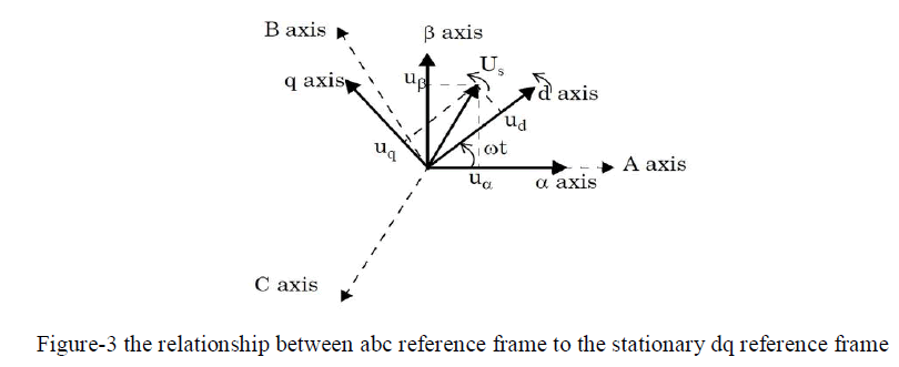
| When these three phase voltages are applied to the AC machine it produces a rotating flux in the air gap of the AC machine. This rotating resultant flux can be represented as a single rotating voltage vector. The magnitude and angle of the rotating vector can be found by means of clark’s transformation as shown in figure-3. This gives the relationship between the abc reference frame to the stationary reference frame [18]. |
 |
 |
| and “f” denotes either a voltage or a current variable. |
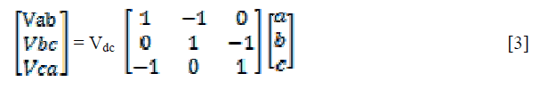
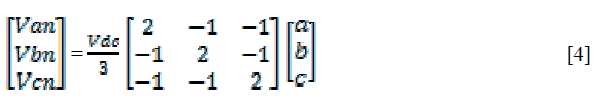
| The relationship between the switching variable vector [a b c] T and the line-to-line voltage vector [Vab Vbc Vca] T is given by |
 |
| Also the relationship between the switching variable vector [a b c] T and the phase voltage vector [Van Vbn Vcn] T is given by |
 |
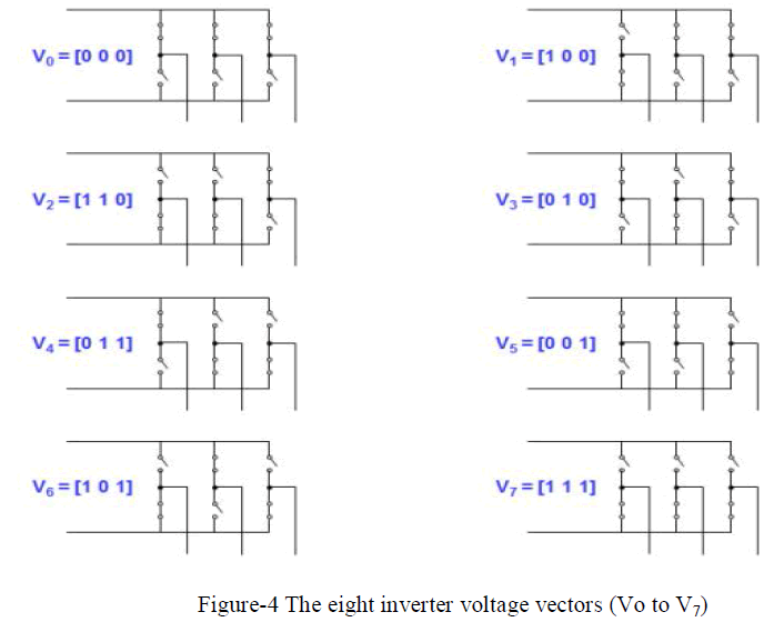
| By referring the figure-2 there are eight possible switching combinations of ON and OFF patterns for the three upper power switches. The ON and OFF states of the lower power devices are opposite to the upper one and so are easily determined once the states of the upper power switches are determined. According to equation-3 and 4, the eight switching vectors, output line to neutral voltage (phase voltage), and output line to line voltages in turns of DC link Vdc are given in the table- 1. The figure-4 shows the eight inverter voltage vectors (V0 to V7). |
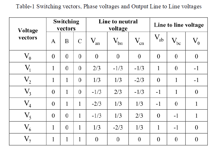 |
| For 180° mode of operation, there exist six switching states and additionally two more states, which make all three switches of either upper arms or lower arms ON. To code these eight states in binary (one-zero representation), it is required to have three bits (2 3 = 8). And also, as always upper and lower switches are committed in complementary fashion, it is enough to represent the status of either upper or lower arm switches [18]. In the following discussion, status of the upper bridge switches will be represented and the lower switches will it’s complementary. Let "1" denote the switch is ON and "0" denote the switch in OFF. Table-1 gives the details of different phase and line voltages for the eight states. |
 |
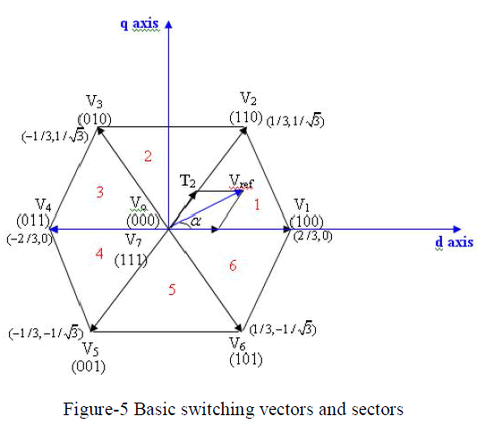
As described in Figure-3. This transformation is equivalent to an orthogonal projection of [a b c] T onto the twodimensional perpendicular to the vector [1 1 1] T (the equivalent d-q plane) in a three-dimensional coordinate system. As a result, six non-zero vectors and two zero vectors are possible. Six non-zero vectors (V 1 to V 6) sharp the axes of a hexagonal as depicted in Figure-3, and supply power to the load. The angle between any adjacent two non-zero vectors is 60 degrees. Meanwhile, two zero vectors (V 0 and V 7) and are at the origin and apply zero voltage to the load. The eight vectors are called the basic space vectors and are denoted by (V 0, V 1, V 2, V 3, V 4, V 5, V 6, V 7). The same transformation can be applied to the desired output voltage to get the desired reference voltage vector,  in the d-q plane. The objective of SVPWM technique is to approximate the reference voltage vector using the eight switching patterns. One simple method of approximation is to generate the average output of the inverter in a small period T to be the same as that of V ref in the same period [6] [13]. The following figure-5 represents the identification of sectors by vector locations. This figure-5 represents all the eight vectors and sectors with 60° displacement with each other. in the d-q plane. The objective of SVPWM technique is to approximate the reference voltage vector using the eight switching patterns. One simple method of approximation is to generate the average output of the inverter in a small period T to be the same as that of V ref in the same period [6] [13]. The following figure-5 represents the identification of sectors by vector locations. This figure-5 represents all the eight vectors and sectors with 60° displacement with each other. |
 |
III. VARIOUS STEPS INVOLVED IN SWITCHING TIME CALCULATION IN SVPWM
|
| By referring the above introductory part of SVPWM principles, the SVPWM can be implemented in the following steps. The first step is to generate three phase waveforms Va, Vb, Vc by referring the equation 1. |
| Va = Vmsinwt |
| Vb = Vmsin(wt-2π/3) |
| Vc = Vmsin(wt-4π/3) |
| Where w = 2πf and f = 50Hz. |
| The second step is transforms abc parameters into dq parameters |
 |
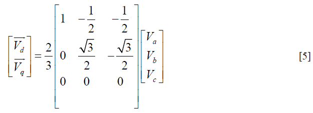 |
| The third step is to calculate Vref magnitude and angle (α) values from equation 5. |
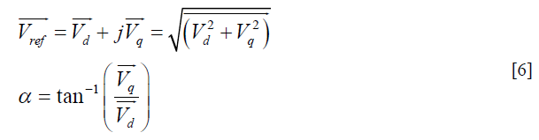 |
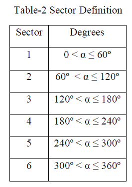
| The fourth step is to identify the sector in which the reference voltage space vector is present. It is necessary to know in which sector the reference output lies in order to determine the switching time and sequence. The identification of the sector where the reference vector is located is straight forward. The phase voltage corresponding to eight switching states: six non-zero vectors and two zero vectors at the origin. Depending on the reference voltages, the angle of the reference vector can be determined the sector as per the table-2 [18]. |
 |
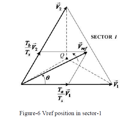
| The fifth step is switching time calculation: to determine the time duration of Ta, Tb and To. Consider the reference vector in sector 1 as shown in figure-6. |
| The volt-second product in sector-1 can be written as |
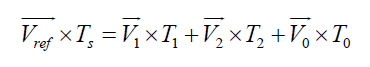 |
| Where |
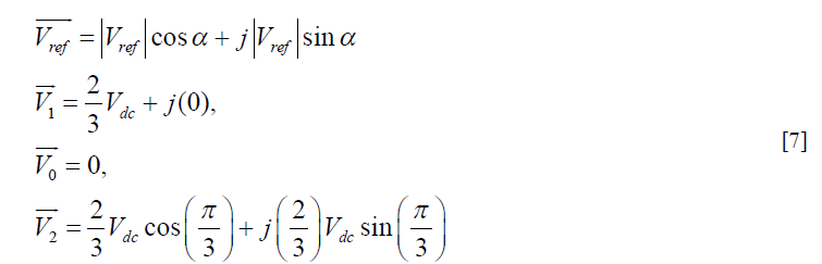 |
| The equation-7 can be written as |
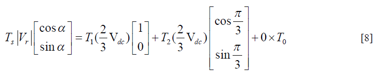 |
| From equation 8 |
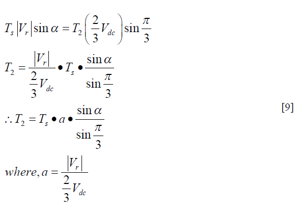 |
 |
| Substitute equation 9 in equation 8 we get a T1 |
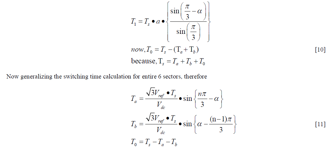 |
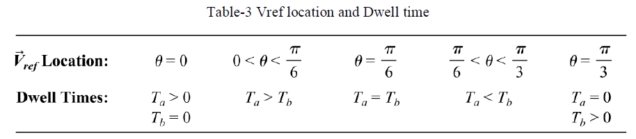
| Where n=1, 2…6 and α = 0 to 60°. The figure-6 shows the reference vector as a combination of adjacent vectors at sector-1. The following table-3 gives the exact location of Vref and its Dwell time in each sector [18]. |
 |
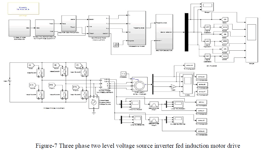
| The detailed circuit diagram for three phase two level voltage source inverter fed induction motor drive is given in figure-7. This circuit diagram is common for all the possible switching sequences. |
IV. THE FIRST POSSIBLE SWITCHING SEQUENCE AND ITS SWITCHING TIME CALCULATIONS
|
| With the space vectors, selected and the switching times or dwell times calculated, the next step is to arrange possible switching sequences. In general the switching sequence design for a given is not unique, but it should satisfy the following two requirements for the minimization of the device switching frequency [13] [14]. |
| a) The transition from one switching state to the next involves only two switches in the same inverter leg, one being switched ON and other being switched OFF. |
| b) The transition of moving from one sector in the space vector diagram to the next requires no or minimum number of switches. |
 |
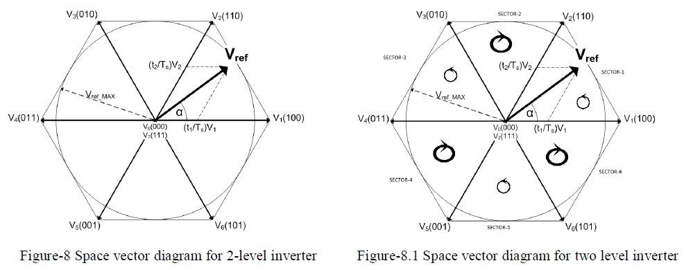
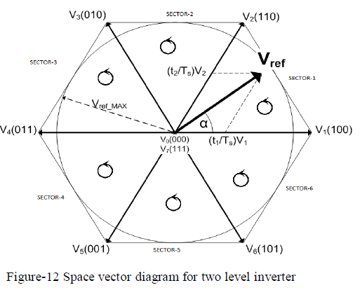
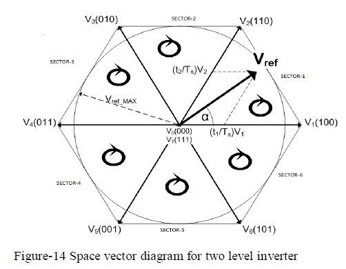
| The figure-8 space vector diagram for two-level inverter shown below should satisfy the above two requirements. This space vector diagram is common to all the four possible switching sequences. Only changes in this space vector diagram are the various possibilities of reference vector rotation in each sectors. |
 |
| The first possible switching sequence in each sector is like, starting with [000] switching sequence and also ends with [000] switching sequence. This will be shown in figure-8.1. The seven segments switching sequence and switching time calculation for each switch for each sector is shown in figure 9.1 to 9.6. |
| Figure 9.1 to 9.6 shows a typical seven segment switching sequence and inverter output waveforms for in each sectors. |
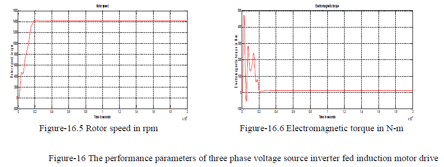
Here is synthesized by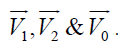 The sampling period Ts is divided into seven segments for the selected vectors. The following can be observed. The dwell time for the seven segments adds up to the sampling periods, Ts = Ta + Tb + T0. The design requirement (a) is satisfied. For instance the transition from [000] to [100] is accomplished by turning S1 ON and S4 OFF, which involves only two switches. The redundant switching state Error! Bookmark not defined. are utilized to reduce the number of switching’s per sampling period. For T0/4 segment in the center of the sampling period, the switching state [111] is selected, whereas for the T0/4 segments on both sides, the state [000] is used. Each of the switches in the inverter turns ON and OFF once per sampling period. The switching frequency fsw of the devices are thus equal to the sampling frequency fsp, ie) fsw = fsp = 1/Ts [13] [14]. The performance parameters of the three phase two level inverters are measured and shown in the figure 16. The sampling period Ts is divided into seven segments for the selected vectors. The following can be observed. The dwell time for the seven segments adds up to the sampling periods, Ts = Ta + Tb + T0. The design requirement (a) is satisfied. For instance the transition from [000] to [100] is accomplished by turning S1 ON and S4 OFF, which involves only two switches. The redundant switching state Error! Bookmark not defined. are utilized to reduce the number of switching’s per sampling period. For T0/4 segment in the center of the sampling period, the switching state [111] is selected, whereas for the T0/4 segments on both sides, the state [000] is used. Each of the switches in the inverter turns ON and OFF once per sampling period. The switching frequency fsw of the devices are thus equal to the sampling frequency fsp, ie) fsw = fsp = 1/Ts [13] [14]. The performance parameters of the three phase two level inverters are measured and shown in the figure 16. |
 |
V. THE SECOND POSSIBLE SWITCHING SEQUENCE AND ITS SWITCHING TIME CALCULATIONS
|
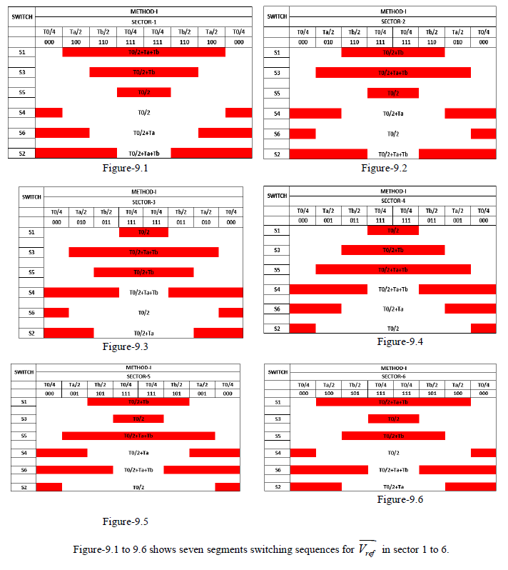
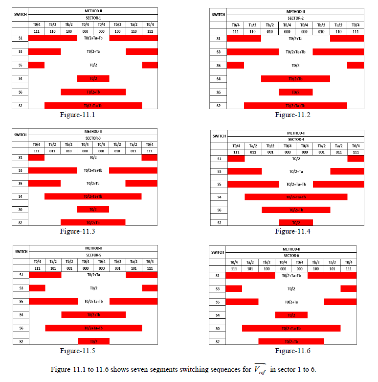
| The first possible switching sequence in each sector is like, starting with [111] switching sequence and also ends with [111] switching sequence. This will be shown in figure-10. |
 |
| The seven segments switching sequence and switching time calculation for each switch for each sector is shown in figure 11.1 to 11.6. Figure 11.1 to 11.6 shows a typical seven segment switching sequence and inverter output waveforms for in each sectors. Here is synthesized by The sampling period Ts is divided into seven segments for the selected vectors. The following can be observed. The dwell time for the seven segments adds up to the sampling periods, Ts = Ta + Tb + T0. The design requirement (a) is satisfied. For instance the transition from [111] to [110] is accomplished by turning S5 ON and S2 OFF, which involves only two switches [13] [14]. The redundant switching state Error! Bookmark not defined. are utilized to reduce the number of switching’s per sampling period. For T0/4 segment in the center of the sampling period, the switching state [000] is selected, whereas for the T0/4 segments on both sides, the state [111] is used. Each of the switches in the inverter turns ON and OFF once per sampling period. The switching frequency fsw of the devices are thus equal to the sampling frequency fsp, ie) fsw = fsp = 1/Ts [13] [14]. The performance parameters of the three phase two level inverters are measured and shown in the figure 16.The sampling period Ts is divided into seven segments for the selected vectors. The following can be observed. The dwell time for the seven segments adds up to the sampling periods, Ts = Ta + Tb + T0. The design requirement (a) is satisfied. For instance the transition from [111] to [110] is accomplished by turning S5 ON and S2 OFF, which involves only two switches [13] [14]. The redundant switching state Error! Bookmark not defined. are utilized to reduce the number of switching’s per sampling period. For T0/4 segment in the center of the sampling period, the switching state [000] is selected, whereas for the T0/4 segments on both sides, the state [111] is used. Each of the switches in the inverter turns ON and OFF once per sampling period. The switching frequency fsw of the devices are thus equal to the sampling frequency fsp, ie) fsw = fsp = 1/Ts [13] [14]. The performance parameters of the three phase two level inverters are measured and shown in the figure 16. |
 |
VI. THE THIRD POSSIBLE SWITCHING SEQUENCE AND ITS SWITCHING TIME CALCULATIONS
|
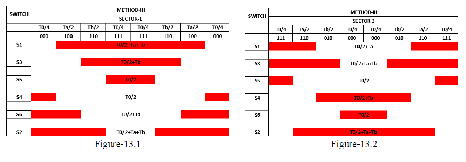
| The third possible switching sequence in each sector is like, starting with [000,111] switching sequence and also ends with [000,111] switching sequence. This will be shown in figure-12. |
 |
| The seven segments switching sequence and switching time calculation for each switch for each sector is shown in figure 13.1 to 13.6. Figure 13.1 to 13.6 shows a typical seven segment switching sequence and inverter output waveforms for in each sectors. Here is synthesized by The sampling period Ts is divided into seven segments for the selected vectors. The following can be observed. |
 |
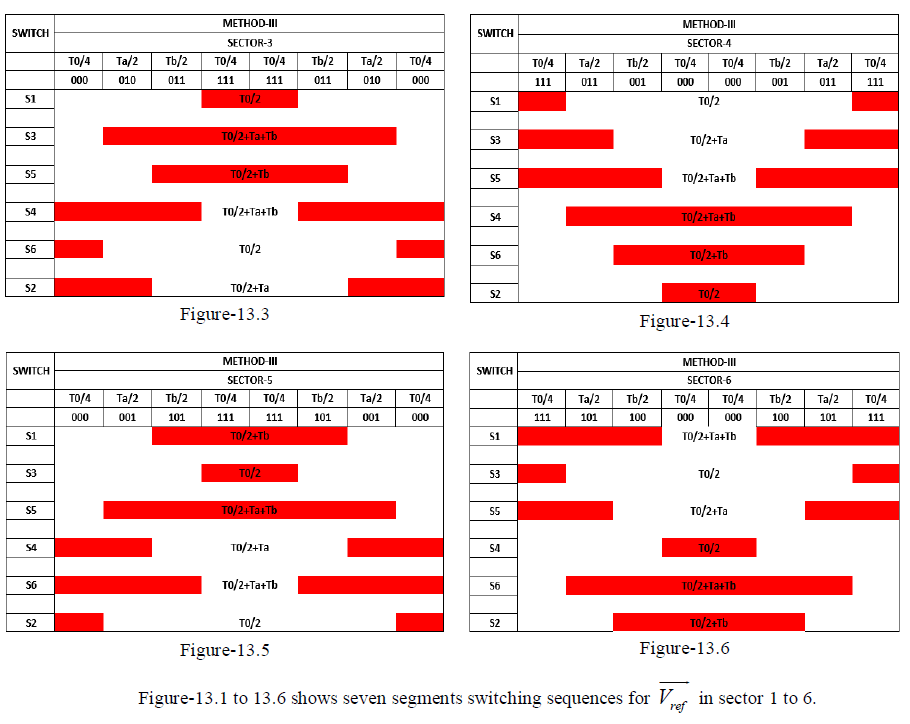 |
| The dwell time for the seven segments adds up to the sampling periods, Ts = Ta + Tb + T0. The design requirement (a) is satisfied. For instance the transition from [000,111] to [100,110] is accomplished by turning S1 ON and S5 OFF, which involves only two switches. The redundant switching state Error! Bookmark not defined. are utilized to reduce the number of switching’s per sampling period. For T0/4 segment in the center of the sampling period, the switching states [000, 111] are selected, whereas for the T0/4 segments on both sides, the states [111,000] are used. Each of the switches in the inverter turns ON and OFF once per sampling period. The switching frequency fsw of the devices are thus equal to the sampling frequency fsp, ie) fsw = fsp = 1/Ts [13] [14].The performance parameters of the three phase two level inverters are measured and shown in the figure 16. |
VII. THE FOURTH POSSIBLE SWITCHING SEQUENCE AND ITS SWITCHING TIME CALCULATIONS
|
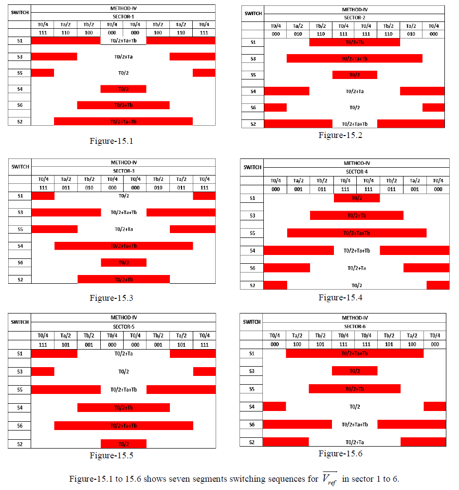
| The fourth possible switching sequence in each sector is like, starting with [111,000] switching sequence and also ends with [111,000] switching sequence. This will be shown in figure-14. The seven segments switching sequence and switching time calculation for each switch for each sector is shown in figure 15.1 to 15.6. Figure 15.1 to 15.6 shows a typical seven segment switching sequence and inverter output waveforms for in each sectors. Here is synthesized by The sampling period Ts is divided into seven segments for the selected vectors. The following can be observed. |
 |
| The dwell time for the seven segments adds up to the sampling periods, Ts = Ta + Tb + T0. The design requirement (a) is satisfied. For instance the transition from [111,000] to [110,011] is accomplished by turning S1 ON and S5 OFF, which involves only two switches. The redundant switching state Error! Bookmark not defined. are utilized to reduce the number of switching’s per sampling period. For T0/4 segment in the center of the sampling period, the switching states [000, 111] are selected, whereas for the T0/4 segments on both sides, the states [111,000] are used. Each of the switches in the inverter turns ON and OFF once per sampling period. The switching frequency fsw of the devices are thus equal to the sampling frequency fsp, ie) fsw = fsp = 1/Ts [13] [14]. The performance parameters of the three phase two level inverters are measured and shown in the figure 16. |
 |
VIII. COMPARATIVE RESULTS OF ALL FOUR POSSIBLE SWITCHING SEQUENCES
|
| The main aim of any modulation technique is to obtain variable output having maximum fundamental component with minimum harmonics. The objective of SVPWM technique is to enhance the fundamental output voltage and the reduction of harmonic content in three phase voltage source inverter. In this paper having different possibilities of switching schemes present in two level SVPWM are compared in terms of THD. The Simulink model has been developed for SVPWM modulated two level three phase voltage source inverter. The simulation work is carried in MATLAB/SIMULINK. |
| The simulation parameters used are; AC input voltage = 440V, fundamental frequency = 50Hz, ODE solver = ode45 (Dormand-Prince), switching frequency = 12 kHz, modulation index = 0.87, Rated power = 3HP, Type of motor = Three phase squirrel cage induction motor, Discrete solver model = forward Euler, Reference frame = Stationary, Stator resistance = 0.4355Ω, Stator inductance = 4mH, Rotor resistance = 0.816Ω, Rotor inductance = 2mH, filter = second order filters. The results for three phase voltage source inverter fed induction motor drive for all the possible switching combinations are given below. |
 |
 |
| The performance of two level SVPWM modulated three phase VSI is analyzed by considering parameters. The comparative statements of each parameter are given below. |
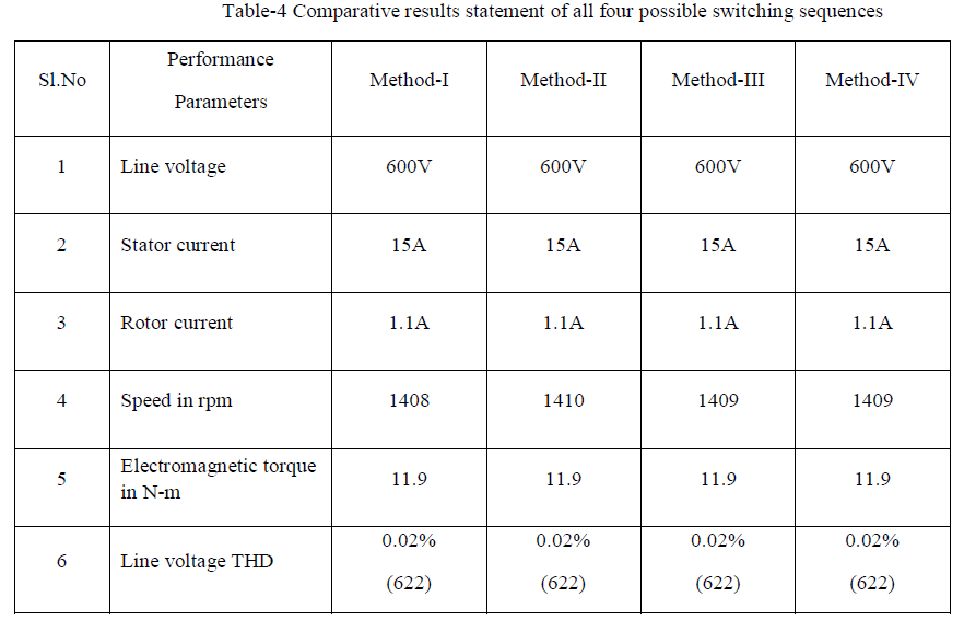 |
| From the comparative result we can conclude like, there is no changes in the performance of three phase VSI fed induction motor drive. We can use any switching sequence for control the speed of three phase VSI fed induction motor drive. The results show clearly all the performance parameters are having the same values in each method of switching sequences. |
IX. SVPWM TECHNIQUE FOR Z-SOURCE AND T-SOURCE INVERTERS
|
| All the above section represents the basic concepts recording SVPWM, the various switching sequence in SVPWM and the performance of 2-level three phase voltage source inverter fed induction motor drive. The same concepts can be represented in the Z - Source inverter (ZSI) and T-Source inverter (TSI) also. The procedure for switching sequence in ZSI and TSI are same as three phase voltage source inverter except the introduction of a shoot though zero state in ZSI. The following subsequent paper should explain these concepts in details. |
X. CONCLUSION
|
| The SVPWM technique can only be applied to a three-phase inverter and it increases the overall system efficiency. The SVPWM is used for controlling the switching of the machine side converter. Advantages of this method include a higher modulation index, lower switching losses, and less harmonic distortion compared to SPWM. Therefore SVPWM research has been widespread in recent years, making it one of the most popular methods for three-phase inverters because it has a higher fundamental voltage output than SPWM for the same DC bus voltage. The SVPWM is significantly better than SPWM by approximately 15.5%. However, the SVPWM technique is complex in implementation, especially in the overmodulation region. But SVPWM technique has become the most popular and important PWM technique for three phases VSI for the control of AC induction. This paper has provided a thorough review of the each technique with a special focus on the operation of SVPWM in all the four possible switching sequences. In this paper, Simulink models for all four switching sequences has been developed and tested in the MATLAB/SIMULINK environment. This paper discusses the advantages and drawbacks of each switching sequence and their simulation results are compared and analyzed by plotting the output harmonic spectra of various output voltages and computing their total harmonic distortions (THD). As seen from the simulation results the DC bus utilization will be same for all the four possible switching sequences, but the THD will be varied for every switching sequence. From the simulation results we can come to the conclusion like, there is no changes in the performance of three phase VSI fed induction motor drive. We can use any switching sequence for control the speed of three phase VSI fed induction motor drive. The results show clearly all the performance parameters are having the same values in each method of switching sequences. In the future researches there are some possibilities are available for implementing the same switching sequence in three phase ZSI and TSI. Definitely the performance of ZSI and TSI will be varied with respect to its different switching sequences. |
References
|
- J. Holtz, “Pulse Width Modulation – A Survey”, IEEE Transaction on Industrial Electronics., Vol. 39, no. 5, Dec. 1992, pp. 410-420.
- Granado, J., Harley, R.G., Giana, G, “Understanding and Designing a Space Vector Pulse-Width-Modulator to Control a Three PhaseInverter”, Transaction Of the SAIEEE (1989), Vol.80, Sept.1989, pp. 29-37.
- Holtz, J. (1994). “Pulse Width Modulation for Electronic Power Conversion”, Proceedings of the IEEE, Vol.82, No.8, pp. 1194-1214.
- Holms, D.G. (1996). “The Significance of Zero Space Vector Placements for Carrier-Based PWM Schemes”, IEEE Transactions onIndustry Applications, Vol. 32, No. 5, pp. 1122-1129.
- Zhai, L. and Li, H. (2008) “Modeling and Simulation of SVPWM Control System of Induction Motor in Electric Vehicle”, IEEEInternational Conferences on Automation and Logistics, pp. 2026-2030.
- Bose, B. K, 2002, “Modern Power Electronics and AC Drives”, Prentice Hall PTR, New Jersey.
- J. H. Seo, C. H. Choi, and D.S. Hyun, “A new simplified space-vector pwm method for three-level inverters,” IEEE Transaction onPower Electronics, vol. 16, no. 4, pp. 545-550, Jul. 2001.
- T. Bruckner and D. G. Holmes, “Optimal pulse-width modulation for three-level inverters,” IEEE Transaction on Power Electronics,vol. 1, no. 20, pp. 82-89, Jan. 2005.
- O. Ogasawara, H. Akagi, and A. Nabae, “A Novel PWM Scheme of Voltage Source Inverters Based on Space Vector Theory,” EPEEurop. Conference in Power Electronics and Applications, Aachen, 1989, pp-1197-1202.Copyright to IJAREEIE www.ijareeie.com 10104
- G. S. Buja and G. B. Indri, “ Optimal Pulse width Modulation for Feeding AC Motors”, IEEE Transaction on Industrial Applications,Vol. IA-13, No. 1, Jan. /Feb. 1977, pp. 38-44.
- A. Nabae, S. Ogasawara and H. Akagi, “A Novel Control Scheme for PWM Controlled Inverters”, IEEE Industrial ApplicationsSociety Annual Meeting, Toronto, 1985, pp. 473-478.
- K. Vinothkumar et.al, “Simulation and Comparison of SPWM and SVPWM Control for Three Phase Inverter”, ARPN Journal ofEngineering and Applied Sciences, Vol. 5, No. 7, July-2010.
- D. G. Holmes and T. A. Lipo. 2003. “Pulse Width Modulation for Power Converters: Principles and Practice”. New Jersey: IEEEPress, Wiley Publications, New York, USA.
- Bin Wu “High-Power Converters and AC Drives”, IEEE Press, Wiley-Interscience. pp. 95-117.
- Zhou, K., and Wang, D. “Relationship between space-vector modulation and three-phase carrier-based PWM: A comprehensiveanalysis”, IEEE Trans. Industrial Electronics., 2002, 49-1, pp. 186-196.
- N. Mohan, T. R. Undeland, W. P. Robbins, “Power Electronic Converters, Applications, and Design”, John Wiley & Sons, Inc. MediaEnhanced Third Edition.
- Phuong Hue Tran, “Matlab/Simulink implementation and analysis of three pulse-width-modulation (PWM) techniques”, Master ofScience in Electrical Engineering, Boise State University, May 2012.
- Jin-Woo Jung, “Space Vector PWM Inverter”, Ph.D., Thesis, Department of Electrical and Computer Engineering, The Ohio StateUniversity, Feb.20, 2005.
- Muhammad H. Rashid, “Power Electronics Handbook”, Academic Press Series in Engineering.
|