Keywords
|
| Multicell,SPWMTechnique,SVPWM Technique,Switched Inductor, Z-Source Inverter, |
I. INTRODUCTION
|
| Voltage and Current type can surely added by connecting appropriate DC- DC converters to the traditional inverters, which is the most commercial way of approach because of its simple structure, Z-Source inverters has actively progressed in terms of modulation, controlling and modelling [2]-[5],component size has been addressed with their applications[7]-[9]. The Z-Source inverters conversion gains are infinite theoretically with practical issues like high semiconductor stresses and spectral performances are poor and constraint are those which are in between modulation index and shoot through duration by the Z-source Inverters are experienced. |
| Each technique has its advantages and disadvantages that might applicable for specified applications The final decision on which to select is therefore dependent on problems under considerations and preferences. The various developments related to DC to AC inverters are found in the literature. Among this the noticeable is Multicell and Single cell Zsource inverter whose single cell type is shown in Fig.1[1], where it provides sinusoidal input and output waveform with minimum higher order harmonics and no sub harmonics. The new Z-source type networks consists of two inductors and two capacitors are connected to the three phase bridges as shown in Fig.1, |
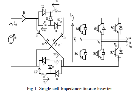 |
| The ZSI advantages uses the ST states to boost DC link voltage by gating on both the upper and lower switches of phase leg, where the Electromagnetic Interference will not destroy the circuit. However a more reliable single stage conversion for both buck and boost operation can obtained. |
II. IMPROVED MULTICELL SL TOPOLOGY
|
| The improved Multicell Switched Inductor Topology is shown in Fig 2. Where the cell structure is shown. It comprises of one inductor Ln and three diodes D3n-1, D3n-2 and D3n for the nth cell. This cell will be duplicated for 2N times (where N is an Integer) divided equally between the upper and lower sides, Note that the inductors L2N+1 and L2N+2 are not included in the cells , but rather shown as the original two inductors as shown in Fig.1. It thus appears that the style of forming the improved cells allows the Switched Inductor type to be viewed as adding extra cells to the original two inductors rather than to replace them[10]. |
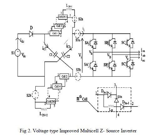 |
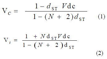
| These cells must introduce additional inductors in parallel during shoot- through charging and more inductors in series during nonshoot- through discharging. Features and expressions for the two processes are summarized as follows. Shoot-through: By turning on two switches from the same phase leg of the VSI bridge. That causes diodes D and D3n to turn OFF, while diodes D3n-1 and D 3n-2 conduct. All inductors are then charged in parallel by the two Z-Source capacitors, giving rise to common inductive voltage VL = VC. Nonshoot –through: By representing one of the traditional active VSI states. In this state, diodes D and D3n conduct, while diodes D3n-1 and D3n-2 block. All inductors then discharge in series to the external AC load, whose common inductive voltage is written as VL= (Vdc – Vc)/(N+1), where N+1 is the number of inductors in the upper or lower cascaded block. Averaging VL over a switching period to zero then gives the following expression for governing the Improved multicell ZSI |
 |
 |
| The boost factor is given by B= (1+NdST) ÃÅø (1-(N+2)dST ), which will be made higher than the previous gains by adding more cells. The desired gain is also arrived at a reduced shoot-through duration whose limit is given as dST <1/(N+2) is derived by setting the denominator of (3) to greater than zero. That allows a higher modulation ratio to be used since M ≤ 1.15(1- dST )Better utilization of DC- link, stress with lower components and better performance linked to a high M can be achieved[6]. With these characteristics, with this improved switched inductor topology is likely to find applications in renewable or other clean energy industry, where high boosting gain for grid interfacing is usually needed[11]. |
III.THREE PHASE VOLTAGE SOURCE INVERTER
|
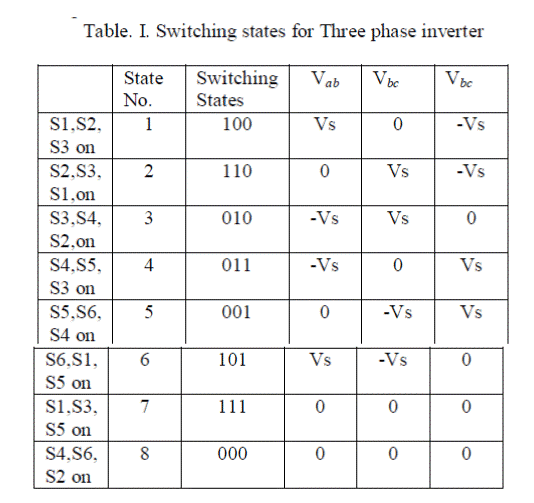
| The circuit diagram for three phase VSI is shown in Fig.3 and the eight valid switching states are given in Table.1. As in single phase the switches of same leg of the inverter( S1 and S4, S3 and S6,S5 and S2) cannot be switched on simultaneously because this will result in a short circuit across the DC link voltage supply. Similarly, In order to avoid undefined states in VSI, and thus undefined AC output line voltages, the switches of any leg of inverter cannot be switched off simultaneously as this will result in voltages that will depend upon the respective line current polarity. |
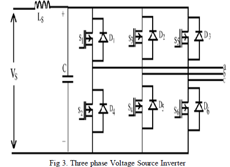 |
| During the switching states 7 & 8 the AC current freewheel through either the upper or lower component which produces zero AC line Voltage. The remaining states from 1 to 6 produces non zero AC output voltages. The inverter moves from one state to another to produce a required voltage waveform. Thus resulting AC output, line voltages consist of discrete values of voltages that are Vs,0 and –Vs . |
 |
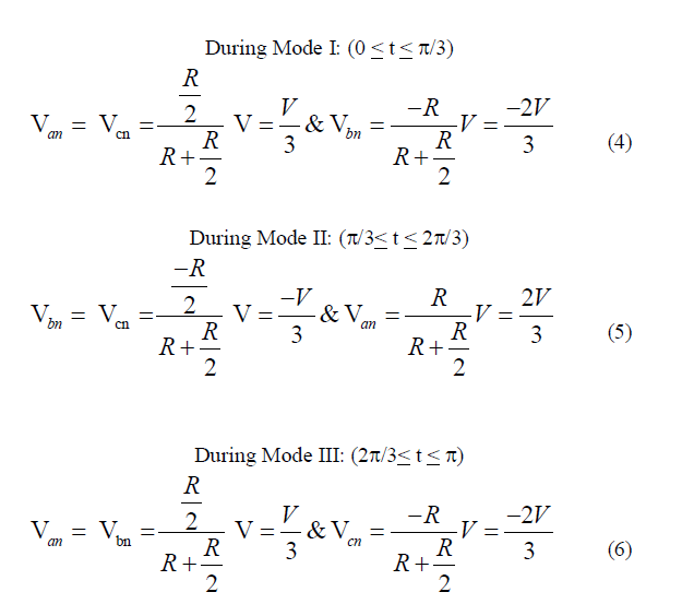
| The line to neutral voltage must be determined to find the line (or phase) current. There are three modes of operation in a half-cycle and the expression for each mode will be given below, |
 |
IV. SIUSOIDAL PULSE WIDTH MODULATION
|
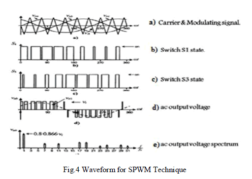
| The generation of gating signals with sinusoidal PWM is shown in Fig.4. There are three sinusoidal reference waves (Vra, Vrb and Vrc) each shifted by 120°. A carrier wave is compared with the reference signal corresponding to a phase to generate the gating signals for that phase. Comparing the carrier signal Vcr with the reference phases Vra, Vrb and Vcr will produce S1 and S3 respectively as shown in Fig.4b. The instantaneous line to line output voltage is Vab = Vs(S1- S3).The output voltage as shown in Fig.4d is generated by eliminating the condition that two switching devices in the same arm cannot conduct at the same time. The normalized carrier frequency should be odd multiple of three. Thus all phase voltages (Van, Vbn, Vcn) are identical but 120° out of phase without even harmonics, moreover harmonics at frequencies multiple of three are identical in amplitude and phase in all phases. |
 |
| For instance, if the ninth harmonic voltage in phase ‘a’ is, |
 |
V. SPACE VECTOR PULSE WIDTH MODULATION TECHNIQUE
|
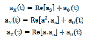
| Space Vector Modulation(SVM) is an algorithm for the control of Pulse Width Modulation(PWM). It is used for the creation of alternating waveform (AC) .It is mostly used in inverters, Three phase AC powered motors. There are various types of SVM that result in different quality and computational requirements. One active area of development in the reduction of Total Harmonic Distortion(THD) created by the rapid switching inherent to these algorithms. With the increase of levels, traditional approaches of SVM based on five level or seven level inverters are hardly realized. Some modified methods have been proposed to approach the SVM of inverter with any levels. One of them is carrying out the SVM in 60° coordinates. This section will outline this SVM scheme. Any three phase system defined by ax(t), ay(t), az(t) can be represented uniquely by rotating vector as, |
 |
| Given a three phase system, the vector representation is achieved by the following 3/2 transformation: |
 |
| Where (Aα, Aβ) are forming an orthogonal 2-phase system as= Aα+jAβ. A vector can be uniquely defined in the complex plane by these components. The reverse transformation (2/3 transformation) is given by, |
 |
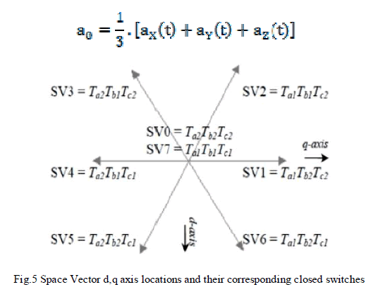 |
| The Space Vector Modulation treats the sinusoidal voltage as a constant amplitude vector rotating at constant frequency. It approximates reference voltage Vref by a combination of eight switching patterns (V0 to V7)[12]. |
VI.SIMULATION AND RESULTS
|
| The MATLAB/ Simulink model of the Multicell Z-Source inverter based SPWM technique with DC to AC inverter is shown in Fig.6 |
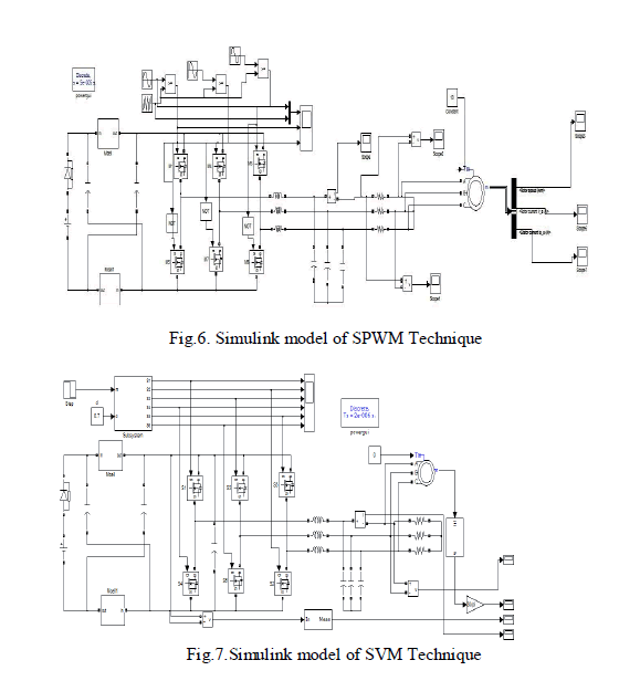 |
| The above Fig..6 and Fig.7 shown for the SPWM Technique and SVM Technique.The values of Z- Source components are L=150μH and C = 1500μF |
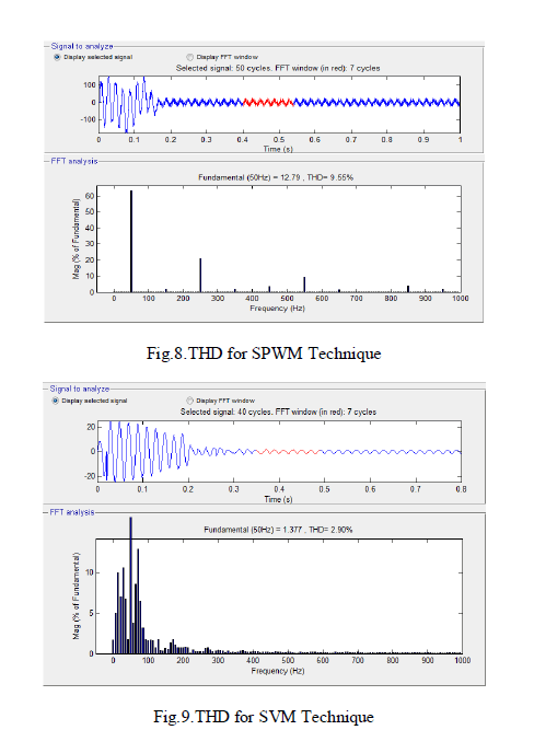 |
| The THD result obtained for stator current with SPWM Technique is shown in Fig.8 and for SVM Technique is shown in Fig.9.It is observed that the THD is 9.55%, The THD level for SVM Technique is 2.90%, which is lower than the SPWM Technique. |
 |
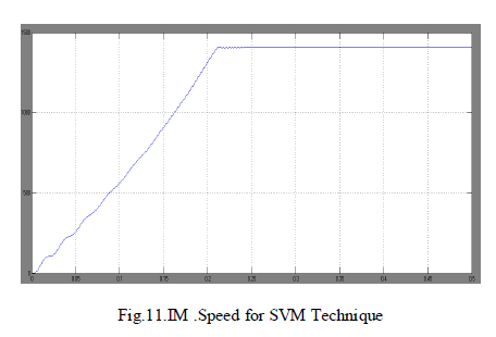 |
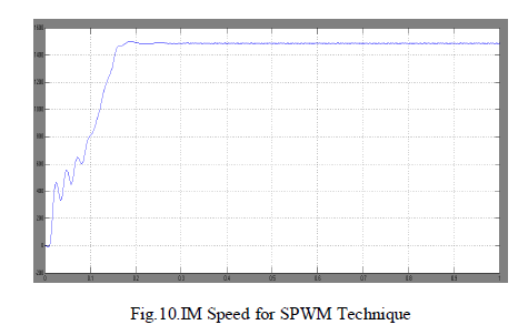
| The achieved speed characteristics of the induction motor for both the technique is shown in the Fig.10 and Fig.11. The dynamic response of the speed is found to be improved in SVPWM technique when compared to SPWM technique with 1500rpm. |
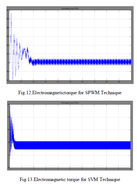 |
| The electromagnetic torque obtained in induction motor is shown in Fig.12 and Fig.13. The torque ripple is observed to be much reduced when SVM technique is used due to reduced harmonic content in the stator current when compare to SPWM. |
VII. CONCLUSION
|
| In is paper Multicell Z-Source Inverter solution for three phase Induction Motor with . The proposed system is compared with SPWM technique. By using SPWM harmonics are more. To overcome this disadvantage SVM Technique is used by using his switching losses are also controlled because of selected switching and harmonics are also controlled and reduced compared to SVM Technique. Finally SPWM and SVM controlled Multicell Z-Source inverter is analyzed by Simulation results are obtained and resulting in stability improvement. |
References
|
- F. Z. Peng, “Z-source inverter,” IEEE Trans. Ind. Appl., Vol. 39, no. 2, pp. 504–510, Mar./Apr. 2003.
- P. C. Loh, D. M.Vilathgamuwa,Y. S. Lai, G. T. Chua, andY.W. Li, “Pulsewidthmodulation of Z-source inverters,” IEEE Trans. Power Electron.,Vol. 20, no. 6, pp. 1346–1355, Nov. 2005.
- J. Liu, J. Hu, and L. Xu, “Dynamic modeling and analysis of Z-source converter—Derivation of ac small signal model and design-orientedanalysis,” IEEE Trans. Power Electron., Vol. 22, no. 5, pp. 1786–1796, Sep. 2007.
- . P.S.Anish, T.ArunSrinivas and M.Sasikumar, Harmonic Reduction in SVPWM Controlled Diode Clamped Multilevel Inverter for Motor Drives(IOSR Journal of Engineering, Vol.2 Issue 1, pp. 170-174, Jan 2012
- D. Li, F. Gao, P. C. Loh, M. Zhu, and F. Blaabjerg, “Hybrid-source impedance networks: Layouts and generalized cascading concepts,” IEEETrans. Power Electron., Vol. 26, no. 7, pp. 2028–2040, Jul. 2011.
- . Kwasinski A., Krein P. T., Chapman P. L., Time Domain Comparison of Pulse-Width Modu-lation Schemes, IEEE Power Electronics Letter,vol.1, no.3, September 2003
- F. Z. Peng, A. Joseph, J.Wang, M. Shen, L. Chen, Z. Pan, E. Ortiz-Rivera, and Y. Huang, “Z-source inverter for motor drives,” IEEE Trans.Power Electron., Vol. 20, no. 4, pp. 857–863, Jul. 2005
- J.-H. Park, H.-G. Kimy, E.-C. Nho, and T.-W. Chun, “Power conditioning system for a grid connected PV power generation using a quasi-Zsourceinverter,” J. Power Electron., Vol. 10, no. 1, pp. 79–84, Jan. 2010.
- D. Cao, S. Jiang, X. Yu, and F. Z. Peng, “Low cost semi-Z-source inverter for single-phase photovoltaic systems,” IEEE Trans. Power Electron.,Vol. 26, no. 12, pp. 3514–3523, Dec. 2011.
- M. Zhu, K. Yu, and F. L. Luo, “Switched inductor Z-source inverter,” IEEE Trans. Power Electron., Vol. 25, no. 8, pp. 2150–2158, Aug. 2010.
- M. Zhu, D. Li, P. C. Loh, and F. Blaabjerg, “Tapped-inductor Z-source inverters with enhanced voltage boost inversion abilities,” in Proc. IEEEInt. Conf. Sustainable Energy Technol, pp. 1–6. Dec. 2010
- M. Savio and M. Sasikumar “Space Vector Control Scheme of Three Level ZSI Applied to Wind Energy Systems” IJE Transactions Vol. 25,No. 4, pp 275-282, Dec 201.
|