International Journal of Advanced Research in Electrical, Electronics and Instrumentation Engineering
ISSN ONLINE(2278-8875) PRINT (2320-3765)
ISSN ONLINE(2278-8875) PRINT (2320-3765)
Se-Young Choi1, Kyoon Choi2 and Sung Jin Kim3
|
| Related article at Pubmed, Scholar Google |
Visit for more related articles at International Journal of Advanced Research in Electrical, Electronics and Instrumentation Engineering
Al-doped ZnO Thin Films were deposited on glass Substrates at room temperature by Ion beam assisted Molecular Beam Epitaxy deposition. Crystal linty, Microstructure, Surface Roughness, electrical and optical prosperities of thin films were investigated as function of deposition parameter such as ion energy. The microstructure of Al-doped ZnO Crystalline films on amorphous glass Substrates were closely related to oxygen Ion energy bombardment on the growing Surface of the film may be divided into two Categories : 1) The enhancement of atom Mobility at low energetic Ion bombardment. 2) The surface damage by radiation damage at high energetic Ion bombardment. Large of the sizes grain structure was obtained in the films deposited at 300eV. With Increasing the Ion energy to 600eV, large of the sizes grain structure was changed into the grain structure. At the high energy Ion bombardment of 600eV, however, the only grain structure was observed. The electrical properties of the deposited films were significantly related to the change of microstructure and Crystal linty. The Al-doped ZnO films with the large of the sizes grain structure have the good electrical properties than those with the grain structure, because the grain boundary scattering was reduced in the large sizes structure compare with the small size grains. The optical photoluminescence of Al-doped ZnO Films was dependent on a grain size.
Keywords |
| Al-doped ZnO, Ion beam assisted molecular beam epitaxy, transparent conducting oxide |
INTRODUCTION |
| As modern timeâÃâ¬ÃŸs changes into the age of information & communication, the age of multimedia is coming. Accordingly, as development of numerous display devices and optical recording devices accelerates, researches on these materials are now very active along with photo electronics. |
| Especially ever since the light emitting display was successfully realized using GaN in the mid 1990, semiconductor researches on growth of epitaxial thin films and the electro optical properties accelerate, and, recently, researches on new semi-conductor materials as central technologies of display devices and DVD are being carried out in advanced countries such as US and Japan. Among them, the mostly used transparent electrode right now is ITO (indium tin oxide) thin film. Having high transparency in the visible light band (-90% at 550nm), low electrical conductivity (ïýÞ2×10⁻⁴Ωcm), and high work function, ITO (indium tin oxide) is widely used as a transparent electrode in organic EL (OLED), solar cell, and LCD (liquid crystal display). [1] However, the ITO thin film has serious problems such as high production cost of in, its raw material, and property changes due to deterioration in the event of exposure to plasmas. [2-3] |
| Al-doped ZnO is getting attention as a material of next generation semi-conductors to replace GaN. Because the Al-doped ZnO thin film, âÃâ¦Ã¡-âÃâ¦ÃÂ¥ family oxide semi-conductor, has an optical band gap of 3.37eV and high exciton energy (59meV), its oscillation strength is high enough to replace previous GaN (21meV) and ZnSe (20meV). Hence, it is an oxide semi-conductor much studied as optical devices such as LED (light emitting diode) with a good lighting efficiency or LD (laser diode), transparent electrode such as plane display, and ultra-violet light receiving element. In general, the zinc oxide thin film is a high piezoelectric material and has been widely used as piezoelectric crystal element or elastic surface element because of the high photoelectric coefficient and refraction coefficient. [4] Since green emission and near band edge emission (NBE) due to ZnO defects was suggested by Reynolds et al. in 1996 as an emission mechanism similar to the yellow emission and near band edge emission (NBE) due to GaN defects, active researches are under progress on metal-organic chemical Vapor deposition (MOCVD) [5], D.C. and R.F. magnetron sputtering [6], Spray Pyrolysis [7], pulse laser deposition [8]. In general, when a transparent electrode is deposited, the process enhancing electrical and optical properties of a transparent electrode is carried out by heating the board at the range of 200âÃâÃÆ-500âÃâÃÆ, treating the board with oxygen plasma before vapor deposition, or annealing process before vapor deposition. However, this process is hardly applicable as an organic light emitting display or a transparent electrode based on plastic, because it has low electrical conductivity and high transmittance and it is difficult to obtain a transparent electrode by performing in the low temperature process. |
| Recently, there is a growing interest in applying organic substrates instead of widely used glass substrates for liquid crystal display devices by many professor, researcher and so on. Hence, development of a low temperature transparent electrode based on films having flat surface roughness, low electrical conductivity, and high transmittance is still considered a meaningful challenge in application to industry. Currently, a few scientists are carrying out the process of ion beam assisted deposition, to form a transparent electrode at a low temperature and obtain transmittance over 85% and low electrical resistance (ïýÞ2×10⁻⁴Ωcm). [9] |
| IBAD-MBE (Ion beam assisted -Molecular beam epitaxy) is the method that makes use of the ion beam irradiation effect by radiating ions with energy during thin film grows, and has the advantage of being used as an important means to control the physical and chemical properties of the deposited thin film because it is possible to control parameters of ion beam, ion flux, ion beam energy, ion beam types, and ion beam direction independently of the vapor deposition method of thin film.By using ion beam assisted deposition (IBAD), it is the possible to control precisely the final material properties such as microstructure, non-stoichiometry, crystallinity, and hence the film will have high density, smooth morphology and strong adherence between film and substrate.[10] |
| However, in spite of the advantages of the IBAD-MBE reaction, there are only research materials on ZnO oxides by sputtering method or heat oxidation method, but systematic research on manufacturing the Al-doped ZnO thin film using the IBAD-MBE method and ion beam energy conversion effect is very rare. |
| Therefore, in this research, we grew the Al-doped ZnO thin film by the molecular beam deposition making use of the activated oxygen Cold Hollow Cathode, and investigated its crystalizability, optical and electrical properties depending on the ion beam irradiation effect, to find out applicability of the Al-doped ZnO optical element material and, the electrical and optical properties of Al-doped ZnO thin film deposited on glass substrates at room temperature by oxygen ion beam assisted method were investigated. |
EXPERIMENTS |
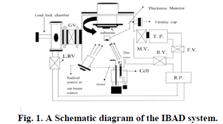
| Al-doped ZnO films were prepared by the Ion beam assisted deposition technique on glass substrates (Corning 7059) by using Al-doped ZnO (2:8) Pellet. The substrates (2âÃËÃâ2 cm) were cleaned in acetone, ethanol and distilled water, sequentially, and dried with nitrogen gas. Prior to deposition, the chamber was evacuated to 10âÃËÃâ10 -8 torr Pa. |
| During the Operating pressure was evacuated to 4âÃËÃâ10 -4 torr Pa, Oxygen partial pressures were controlled at 4âÃËÃâ10 -4 pa and 3âÃËÃâ10 -4 by admitting oxygen gas through a leak valve. In addition, the secondary ion beam energy changed from 0eV to 600eV. After variable process parameters, such as primary Oxygen ion bombarding energy and oxygen ion dose, were held constand plasma current 300mA, 1âÃËÃâ1015 Ion /cm2 , Respectively. The deposition time was adjusted to obtain a film thinness of 100 nm. The thickness was measured from surface profilometer. Almost no change in the film thinness occurred. The optical transmission was measured with a UV-visible spectrophotometer in wavelength from 300nm to 900nm. Surface Morphology of the ZnO Thin film was obtained by using atomic force microscopy (AFM) and Microstructure was examined by scanning electron microscopy (SEM) analysis |
| The structural properties were investigated by X-ray diffraction analysis with a Cu target (40 KV, 300mA). The resistivity of the film was measured by a four-point-probe method, and Hall Mobility was measured by the van der Pauw method. |
 |
RESULT |
| Figure 2 shows the X-ray diffraction (XRD) pattern of the Al-doped ZnO thin film that was deposited as the ion beam irradiation was varied. First of all, the Al-doped ZnO thin film deposited in the amorphous state was analyzed, using the Bragg law and θ/2θ scan, on the crystal plane in the direction parallel to crystal phase and circuit board. For analysis, a Rigaku X-Ray diffractor (RINI/DAX 2500) was used and the analysis conditions were 300KV and 126mA with the measuring speed of 10.000 deg/min, and the used X-Ray was Cuka line with the wavelength of 1.54148âÃâë . The measuring range was determined as 2θ, when the value was set up as 20°Ã¯Ã½Ãž80°.To compare effects of neutral oxygen and ion beam irradiation, vapor deposition was conducted after fixing the circuit board temperature to a room temperature. In the case of the ZnO thin film deposited in the atmosphere of neutral oxygen (Fig. 2(a)), it is possible to see that it grew to multi crystals observed at 2θ= 34.60°as diffraction patterns from the crystal plane on the Al-doped ZnO (002) plane. Compared to this, in the case of the ZnO thin film deposited by irradiating the ion beam coming from oxygen plasma of the IBAD-MBE method, when the ion beam was irradiated to 300 eV, it was possible to observe that the crystal is rearranged in the (002) and (103) plane and preferred oriented in the (103) plane, and when the ion beam was irradiated to 600 eV, the crystal is re arranged in the (002) plane than in the (103) plane. The reason that the preferred crystal plane of the Al-doped ZnO thin film deposited in this ion beam assisted method changes to (002) or (103) is mainly explained by the ion channeling effect [11,12] and anisotropic radiation damage effect [13]. In the case of the ion channeling effect, the incident direction of the assisting ion beam gives the highest effect to the growth of preferred crystal plane, but in this research, the ion channeling effect due to the ion beam irradiation direction can be ignored because the circuit board was rotated when the ZnO thin film was deposited. Instead, the most important elements to the Anisotropic Radiation Damage effect affecting to each crystal plane are energy of the incident assisting ion beam and momentum delivered per unit volume [14].once, if the energy of the assisting ion beam grows, the Radiation Damage effect may appear differently on crystal planes where atomic density and distribution of composition atoms are different. Also, the ion gun used in this experiment has the property that the ion beam current density grows as the ion beam energy increases. Therefore, in a low energy (100 eV) and low current density, the (002) plane where atomic density is the highest (most dense) tolerates the Radiation Damage relatively well, but if energy grows (for example to 300 eV) and current density grows together, effects such as Preferential Sputtering [14], Also affect the growth of preferred crystal plane and, thus, the (103) plane may grow first. This may be explained as follows: When the ZnO thin film is set up on the glass board at a room temperature, stress delivered to the thin film by the discord of lattice constant at the board interface caused deterioration of crystalizability, when many invasive defects of Zn and vacancy defects of O2 disappears due to the ion beam effect and there appear more stoichiometric 1:1 combination of Zn and O2. Due to this, as recrystallization of defects on the ZnO thin film caused by anisotropic radiation damage occur, composition particles move and the ratio of micro crystal gets higher, which improves crystallinity. |
| If the ion beam energy is increased further, in the case of ZnO thin film deposited at a higher ion beam energy than 500 eV, the pattern peak in the (103) plane of the XRD crystal plane gets narrower and half value width gets larger. This is because the high energy of ions arriving at the board surface increases radiation damage due to Re-sputtering at the thin film surface and crystallinity gets lowered. Hence, because of re-sputtering effect due to the assisting ion beam energy at the growth of ZnO, the ZnO thin film deposited at ion energy higher than 500 eV shows relatively low XRD pattern peak than that at the energy of 300 eV. |
| As Kheyrandish et al. considered on the TiN thin film grown in accordance with the ion energy, the shape of thin film grown without ion irradiation is amorphous or randomly oriented, while the thin film irradiated with 300 eV ions showed preferred growth in the (100) direction, and the thin film irradiated with 400 eV energy is restricted to [100]. [15] . It was concluded from these results that ion irradiation to growing thin film can induce preferred growth of thin film, but certain energy may cause thin film disordering. [16] |
| Muller et al. claimed that as incident ions increase surface diffusion and cause local heating and recrystallization, the plane of crystal growth grows or is restricted and as a result rearrangement of crustal occurs, and that the XRD peak crystal plane varies in case the ion beam energy and oxygen partial pressure are different. According to their claim, atoms on the board can move sufficiently by the kinetic energy transformation due to secondary ion collisions. Hence, in the case of thin film irradiated with 600 eV ions, peak decreased compared with the 100 eV and 300 eV cases, because high energy ion collisions chose defects due to radiation damage more than surface mobility increase of deposited atoms. |
| The oxygen ion assist molecular line method can change crystallinity of the Al-doped ZnO thin film and may be very useful for growth of good Al-doped ZnO thin film of C-axis direction depending on the ion beam irradiation. Also, to find out the grain size depending on ion beam effects, Scherer formula was used for the average grain size (t) of the Al-doped ZnO thin film. [17] |
| dgrain = t=0.94λ/Δθcos(θB) (1), |
| where λ denotes x-ray wavelength, Δθ denotes half width value of the (002) or (103) peak, and θB means the Bragg diffraction angle (Radian). λ corresponds to wavelength of the used Cukα x-ray (0.154nm). In Eq. (1), d denotes the size of crystal grain, WFWHM denotes half width of the XRD peak in the (002) plane, λ denotes wavelength of the used Cukα X-ray (0.154nm); θ denotes the Bragg diffraction angle (Radian), respectively. In cases of 0 eV and 600 eV, the (002) plane, and in the case of 300 eV, the (103) plane was used to obtain the average grain size. The thin film average grain size obtained from the above formula was 228âÃâë , 630âÃâë , 195âÃâë , respectively, when 100eV, 300 eV, 600 eV. |
 |
| The Al-doped ZnO thin film thickness was measured using α- step. The influence of ion beam irradiation on the Al-doped ZnO thin film thickness was observed, and to be accurate, after measuring thickness putting the α-step on different positions of the Al-doped ZnO thin film, and this was divided by 3 and average was taken. Figure 3 shows thin film thickness in accordance with ion beam energy. |
| In the case of Al-doped ZnO thin film irradiated by 100 eV ion beam, the thin film thickness was 1854âÃâë in average, in the case of 300 eV ion beam the thin film thickness was 2025âÃâë , and in the case of 600 eV ion beam it grew to 1528âÃâë .To be accurate on these results, side scanning electron microscope was used for another measurement of the Al-doped ZnO thin film thickness, which was 2050âÃâë in the case of 100 eV ion beam irradiation, 2300âÃâë in the case of 300 eV ion beam irradiation, and 1785âÃâë in the case of 600 eV ion beam irradiation. Comparing theα-STEP measurement and the side scanning electron microscope measurement, it was possible to see that the thin film thickness decreases as the ion beam irradiation increases. The reason may be as follows: As the ion beam irradiation grows, nucleus formation at the thin film becomes difficult due to damage by ion irradiation bombing, and even if nucleus is formed, collisions between simply incident ions and stationary atoms increase the differential scattering cross section. Also, due to ion damage within thin film caused by thermal non-equilibrium or energy transfer, the thin film is thinner than the thin film without ion beam irradiation.Actually, according to Daeil Kim and Steven Kim, when the ion beam energy is irradiated to the ITO thin film surface with 200 eV energy, atomâÃâ¬ÃŸs mobility grow due to particle growth and grain size increases. [18] In other words, considering the domain growth model proposed by Kamei et al., the grain size increase on the Al-doped ZnO thin film observed at deposition of 300 eV may be explained as follows: As recrystallization of defects caused by radiation damage occurs by the ion beam irradiation, composition particles begin to move, and as resputtering rate and micro crystal ratio increase depending on the crystal directionality, along with growth of surface mobility of deposited atoms, absorption and diffusion of ions and deposited atoms are strengthened on the thin film surface and the crystallinity due to particle growth is improved. [19] |
 |
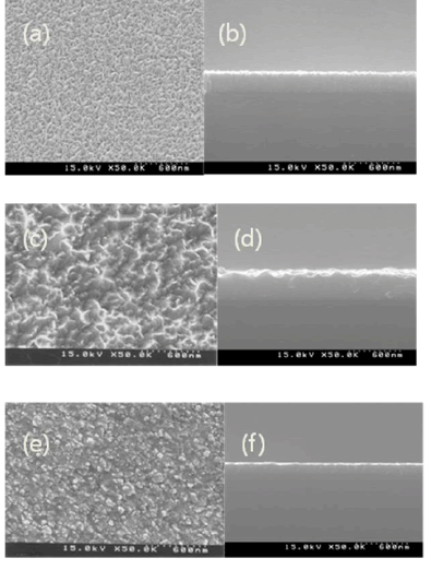 |
| Fig. 4. SEM Photographs of conventionally evaporated ZnO films and cross section of ZnO film on surface glass with varying oxygen ion energies: (a) 100 eV discharge (b) 300eV, (c) 600eV . |
| At this time, deposition variables other than ion energy, such as ion current density, oxygen partial pressure, and board temperature, are constantly maintained at a room temperature, hence, excluded from consideration, and only ion energy is the deposition variable that can change the grain size. Actually, if the ion energy increases, the kinetic energy (EiCos2θ) increases on the thin film. Also, W. Lia* supports the previous basis by claiming that grain size decreases or increases because of the sputter effect caused by ion bombardment. [20] Hence, if 300 eV ion beam is irradiated to the Al-doped ZnO thin film surface, mobility of deposited atoms increase more than damages due to ion collisions and small grains grow to higher grains. Figure 3, (f) is the picture when 600 eV ion beam was irradiated. |
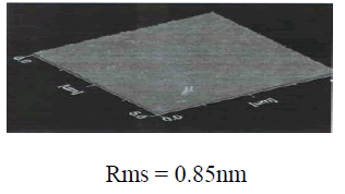
| In the SEM photo, grain size decreases largely, and the Al-doped ZnO grains created at 300 eV are formed in the (103) plane, but at 600 eV, grains that are rearranged in the (002) plane are created. Many surface defects are created as the ion energy increases to 600 eV, and newly generated defects can be predicted to act as a nucleation site by facilitating crystallization, and consequently accelerated nucleation decreases the grain size. Even in the case of H. guchi et.al, they claim that as the ion energy density increases, grain size has a tendency of decreasing, and in the experiment of Screenivas et Al., they claim that as the ion beam irradiation increases, grain size decreases. [21-22]. In PetrovâÃâ¬ÃŸs experiment, this is supported by the fact that as the ion beam irradiation increases, deposited substances are going through renucleation by coalescence of residual Ion irradiation - Induce point defeats. Also, these grounds can be seen while deciphering the SEM picture. Measuring the grain size shows that grain size was 4200âÃâë at 300eV but decreased to 1842âÃâë at 600 eV according to the SEM photo, which supports the resultâÃâ¬ÃŸs reliability.In addition, calculating the XRD peak halfvalue width shows that when ion beam is 300eV, the width is increased higher than when ion beam is 600eV. It can be clearly explained by the example of TiN thin film grown in accordance with the ion energy in Kheyrandish et al. When the ion beam higher than 400eV was irradiated, it was possible to see that thin film growth was limited. Therefore, in the case of 600 eV ion irradiation, it can be predicted that grain growth decreases. From this result it is considered that ion irradiation to the growing thin film can induce preferred growth of film but when high ion beam energy such as 600eV is irradiated, crystal size can be decreased because of disordering from radiation damage in the Al-doped ZnO thin film. This made a conclusion that creation of combination by radiation damage surpassing surface mobility generated new nucleation site and caused creation of small grains. In general, the roughness of a transparent electrode is largely affected by the phase differences and fine structure of the transparent electrode, and affects the optical property.The AZO thin film deposited at a low temperature has a very uniform and flat surface as reflected by the surface roughness of 0.85 nm. However, since the AZO thin film exists in an amorphous form, its transmittance and electrical conductivity is so low that it is not appropriate to be used for the transparent electrode substrate. An experiment shows that the surface roughness is affected by the Ion Beam energy treatment, and its rms value is considered to increase as the Ion beam energy increases. The experimental result shows that in the Ion beam energy treatment at 300eV at the atmosphere of oxygen the sample rms value of the surface roughness is relatively low as 1.4 nm for Ion beam energy annealing from 100eV to 300eV, but at a higher annealing condition, the rms value keep increasing even to the value that is considered inapplicable to electronic elements. The AZO thin film that grew by the sputtering method has incomplete bonds on its surface, such as broken bond, but in the AZO thin film that was post-annealing treated at the oxygen atmosphere, it is considered that broken bonds are reduced due to the oxygen absorption on its surface and crystal particles are re-crystallized very uniformly to achieve a relatively low roughness. [23] With the increase of Ion beam energy, the rms nearly maintains constant.For a high surface roughness, there is a high chance that poor pixels may appear, and for a high rms roughness value, etching can be problematic due to diffused reflection to light exposure and at the same time there can be dark spots on the surface due to the concentration of the applied electric power. [24] |
| Hence, if the surface roughness increases, scattering of the incident light into the thin film also increases, which deteriorates the optical property of visible light. [25]. Therefore, the regulation of the dense particles and rms is considered to be important in the manufacture of touch panel or OLED. As a result of the experiment, the sample that was Ion beam energy treated at 300eV at the oxygen atmosphere has a potential to be a good element, because it is not expected to exhibit these problems at manufacture of Processing. |
 |
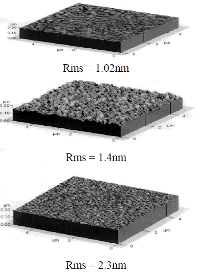 |
| Fig. 5. AFM images and values of the surface roughness of the conventionally evaporated ZnO film in oxygen ion environment and the Zno films deposited at (a) 100eV, (b) 300eV, (c) 600eV. |
| Irradiating oxygen ion assisted molecular beam, the Al-doped ZnO thin film PL properties were studied while fixing plasma discharge current to 300mA, changing ion beam voltage from 100 eV to 600 eV, and the result is seen in Fig 7. This Al-doped ZnO thin film PL measurement is measured with He-Cod laser (λ=325nm). |
| As seen from Fig 7, it is observed that Al-doped ZnO thin film radiates in the ultraviolet, green, and orange regions (378nm~620nm). |
| Al-doped ZnO thin films irradiating in the ultraviolet and visible light regions are also observed in the research of Studeninkin. Al-doped ZnO thin filmâÃâ¬ÃŸs ultraviolet irradiation seems to correspond to the lighting band gap and the result shows that when 300 eV ion beam energy was irradiated, through research of Vanheusdend, green irradiation in the visible light region comes from oxygen lightâÃâ¬ÃŸs defects in the Al-doped ZnO thin film. According to previous researches, peak near 378 nm is a peak from excitonic reunion [26] in Near Band Edge (NBE) of ZnO thin film, wide peak near 520 nm mainly corresponds to Deep Level Emission (DLE) caused by oxygen vacancy (VO) and interstitial zinc(Zni)âÃâ¬ÃŸs defects. [27] Also, orange emission near 650 nm is known to be main lighting center coming from defects of oxygen vacancy. [28] As considered in the XRD spectrum from previous passage, when the assisted ion beam energy is 100eV, it is the case of (002) plane being preferred growth plane and ZnO crystalâÃâ¬ÃŸs c-axis growing perpendicular to the board, and when the energy is 300eV, it is the case of (103) plane being the preferred growth plane and the crystal a-axis growing perpendicular to the board. Therefore, in accordance with the direction of preferred growth crystal plane, the ZnO thin film PL properties can be different, as previously reported from Wang et al. [29] .In this experiment, ion beam was irradiated with the energy of 100 eV, 300 eV, 600 eV, respectively, and its lighting properties were studied. In the result, the value of lighting peak, at each of 378nm, 520nm, 650nm, was different. The reason why PL properties are different in accordance with the preferred growth crystal plane of ZnO thin film is that on each different crystal plane, assisted ion beamâÃâ¬ÃŸs Radiation Damage effect is different, making deposited filmâÃâ¬ÃŸs defect different. In addition, according to research of Korsunska et al. [30] on 520 nm-centered peak, green emission at near 520 nm is a result of defect from zinc interstitial, and orange emission at near 650nm is main lighting center of defect from oxygen vacancy, but it was reported that depending on the ZnO thin film growth method and disposal of the grown film, defects that play major roles in lighting can be different. [31] When the ion beam energy is increased to 300eV, the ZnO thin film which was treated by heat in this temperature is considered to have the nearest stoichiometric construction, judging from the large peak in UV region and the smallest peak in the green light region. However, when the energy was increased to 300eV, the green light peak also showed an increase. This is considered to happen because even though the number of Zn molecules combining with oxygen molecule increases, there are more defects along with molecular size increase due to increase in atomic mobility coming from the energy irradiation effect. The reason why wide peak appears in the wide section of PL spectrum is non-homogenous distribution of defects in the deposited thin film. [32, 33]. |
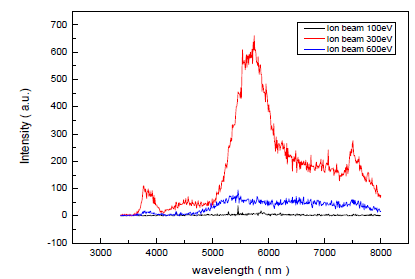 |
| Fig. 6. PL spectra of the conventionally evaporated ZnO film in oxygen environment and the ZnO films with changing oxygen ion beam energy for (a) 100eV,(b) 300 eV ,(c) 600 eV |
| Figure. 7 shows the graph of measured transmittance T(λ) of the Al-doped ZnO thin film by oxygen ion assisted molecular beam deposition in accordance with heat deposition and ion energy. Measurement was performed between the wavelength ranges of 200nm to 800nm. According to the result, measurement of the Aldoped ZnO thin film without ion beam irradiation shows low transmittance less than 80%. The Al-doped ZnO thin film with heat deposition only shows transmittance less than 80% and cannot be used as a transparent electrode, and is created usually in the amorphous state or as minute crystal grain type, which decreases carrier mobility and, thus, electric conductivity, and this represents thin film state unsuitable for LCD or organic EL. Exact cause cannot be known, but it is speculated to be oxygen shortage. However, in the case of Al-doped ZnO thin film by the oxygen ion assisted molecular beam deposition, it has higher transmittance than simple heat deposited thin film. In cases of thin films irradiated with the energy of 100eV and 300eV, transmittance is from 80% to 88% or higher. The Al-doped ZnO thin film irradiated with 300 eV energy has high transmittance according to experiment, because the oxygen rate increases as the deposited Zn atom surface mobility increases. P.Sagar et al. also showed a similar result. [34].However, in the case of thin film irradiated with 600 eV ion beam, transmittance is about 80%. In the equivalent condition that every deposited film is about 100 nm, the fact that thin film irradiated with 600 eV ion beam has low transmittance can be attributed to scattering event occurred from relatively rough surface. That is, when the ion beam energy is increased, the AFM surface roughness increases as well, and this thickens the film and consequently affects optical transmittance. Simultaneously, re-growth of micro particle, grain boundaryâÃâ¬ÃŸs influence, decrease of Oxygen Vacancy and Zn interstitial concentration, and decrease of carrier concentration all act as AZO film donor, and thus the AZO thin film optical transmittance decreases by impurity scattering effect. |
 |
| Fig. 7. Optical transmittance curves of the ion beam assist deposition (IBAD) AZO films prepared with various Ion beam energy. |
| Figure 8 is the result of non-resistance measurement of the ion assisted deposited Al-doped ZnO thin film. Generally, the Al-doped ZnOâÃâ¬ÃŸs non-resistance is determined by the number of carriers and mobility, and the number of carriers is determined by the oxygen content and mobility is determined by the film microstructure. Therefore, crystal microstructure in the Al-doped ZnO thin film acts as a very important factor in conductivity. In order to create a low-temperature crystallization transparent electrode that can be applied to plastic boards, properties of the Al-doped ZnO thin film were studied by changing the ion beam irradiation energy using oxygen-ion assisted molecular beam, and properties of the thin film as a transparent conductive film were investigated. When the ion beam energy was increased to each of 100 eV, 300 eV, 600 eV, microstructures changed as observed previously, and electrical properties also changed. Electric properties of the ZnO thin film are reported to be affected by deposition process, chemical and physical state of deposited condition, and crystal structure. [26] Thin filmâÃâ¬ÃŸs molecular growth factor formed in accordance with change in crystallizability and oxygen ion beam irradiation largely affects characteristics of electric changes in this experiment. After growth, electrical non-resistance, carrier concentration, and charge mobility of the Al-doped ZnO thin film irradiated with 100eV ion beam was 5×10⁻³Ωcm, 4.11×1019cm-3, 13.09cm2V-1S-1, respectively. In the Al-doped ZnO thin film with the ion beam energy increased to 300eV, electrical non-resistance and carrier concentration were increased to 1.10×10⁻⁴Ωcm and 5.71×1020cm-3, and charge mobility was increased to 1021m2V-1S-1. When the ion energy was increased to 600eV, electrical non-resistance was 7×10⁻³Ωcm, carrier concentration was 9.11×1019cm-3, and charge mobility was 7.09cm2V-1S-1. In the Al-doped ZnO thin film, electrical conductivity is due to free electrons supplied from oxygen vacancy in the nonstoichiometric theory. Generally, oxygen vacancy, as a doubly ionized donor, contributes two electrons maximally. |
| OïýÃËO→VOâÃËÃâ¢Ã¢ÃËÃ⢠+ 2e- + 1/2 O2 (g) |
| These changes of carrier concentration and mobility are considered to be originated from the defect chemical structure of AZO. In this reaction, the less the oxygen partial pressure is, the faster the forward reaction occurs. In consequence, it is thought that more tin can be included in the AZO grid, and accompanying free electrons increase the carrier concentration. On the contrary, mobility typically increases in parallel with increase in heat treatment time. This phenomenon is usually explained by grain boundaryâÃâ¬ÃŸs decrease caused by grain growth. |
| Generally, electron concentration of the Al-doped ZnO thin film increases in accordance with nonstoichiometry or oxygen vacancy. However, according to the result, when the ion beam energy was increased from 100 eV to 300 eV, actual electron concentration found to be higher at 300eV.Therefore, electron concentration decrease in accordance with ion energy concentration is not fully explained by nonstoichiometry. Apart from Oxygen Vacancy, electron concentration is also affected by structural defects, especially by grain boundary. On the SEM picture observed previously, Al-doped ZnO thin film observed at 600 eV increases grain boundary density that can act as trap for free electrons, and therefore, it is thought to be composed of small size grains. |
| As its basis, Higuchi et al. claimed that as domain boundary acts as potential barrier in the domain structure, grain boundary acts as potential barrier for electron movement in the grain structure. [35] |
| When the substance crystallographic properties are similar, factors that affect electrical non-resistance are Carrier Concentration and Mobility. In this research, it may be concluded that electrical properties get better by changes of Carrier Concentration.That is, ion beam irradiation affects changes in microstructure, and can control growth and size of molecules. The fact that 300 eV-irradiated thin film with domain structure, which has a small boundary density and can trap electrons or be applied as barrier for electron movement has better electron concentration than 600 eV-irradiated thin film with grain structure is thought to be related to domain formation and growth of domain size. The reason is that electron boundary scatterings decrease because the particle size is larger and grain boundary density is lower than other thin films irradiated differently. When 300 eV ion beam was irradiated, electrical properties were the same type as the result that formed the biggest microstructure particle in the FE-SEM result. Therefore, the Al-doped ZnO thin film influenced by ion beam irradiation might be governed by carrier concentration rather than mobility. However, when 600 eV ion beam was irradiated, strong intensity, ion beam damage, and carrier scattering decreased particle size and thin film thickness, which in turn degraded electrical properties. This showed tendency of decreasing molecular concentration as the ion beam energy increased, and this may be explained as follows: Zn ions, impurities, and re-creation of the ZnO thin film due to ion beam damage caused creation of Zn vacancies. These decreased the number of electrical electrons, and acted as trap centers that stop electron movement because of grain boundaryâÃâ¬ÃŸs recreation, to decrease carrier concentration. Although exact cause is not known, as oxygen vacancies that originally existed under the atmosphere of O2 are filled, the amount of Carrier Concentration decreases. And, at the same time, vacancy formation from rebound atoms increases as the ion beam energy increases, which means that radiation damage increases. Therefore, in the case of Al-doped ZnO irradiated with 600eV ions, it is thought that excessive energy causes surface damage and creates defects, and grain structure is created by increase of nucleation site. This is because excessive energy gives many defects to thin film growing by oxygen ion irradiation. According to the result, to effectively obtain a thin film that has the Al transmittance and conductivity of Al-doped ZnO thin film, it is concluded that ion beam energy should be controlled to below 500 eV and moved to a low kinetic energy zone. These results show that electrical properties of the Al-doped ZnO thin film can be applied to transparent electrodes by controlling ion beam energy. |
 |
| Fig. 8. Dependence of the electrical properties (resistivity, Hall mobility and carrier concentration) of ZnO thin films after different Ion beam energy condition (100eV, 300eV, 600eV) |
CONCLUSION |
| 1. It was verified that the Al-doped ZnO thin film, deposited by varying the oxygen ion assisting beam, shows different direction of preferred growth crystal plane, penetration ratio, and PL property depending on the ion assisting beam energy. When deposited by oxygen ion assistance molecular beam, the deposited microstructure was transformed to grain structure as the oxygen ion energy is changed from 100 eV to 600 eV at a room temperature of the board. When the oxygen ion energy was 300eV, lower than 500eV, the initial effect of ion irradiation on the thin film was surface mobility. As the oxygen ion energy increased, damages on the growing thin film increased, and the microstructure changed into the grain structure because of surface defects that came from the damages. |
| 2. Roughness of the deposited Al-doped ZnO thin film showed close relevance to changes of the microstructure. The thin film with grain structure that has grown on the surface due to ion beam irradiation showed enhanced optical transmission compared to the thin film with grain structure. |
| 3. Electrical non-resistance of the deposited Al-doped ZnO thin film depended highly on changes of the microstructure that depended on ion beam irradiation. A thin film that has large grain as its structure shows better electron mobility and electron concentration, and this is because grain boundary scattering decreases due to particle size growth and ion beam irradiation. Therefore, it is concluded that having a microstructure with large grain structure is optically and electrically desirable at the time of manufacturing the Al-doped ZnO thin film using oxygen ion molecular beam, and this may also be applied to the experiment of doping other substances on the Al-ZnO thin film. |
References |
|