ISSN ONLINE(2278-8875) PRINT (2320-3765)
ISSN ONLINE(2278-8875) PRINT (2320-3765)
A. Timoumi1,2
|
| Related article at Pubmed, Scholar Google |
Visit for more related articles at International Journal of Advanced Research in Electrical, Electronics and Instrumentation Engineering
In2S3 films have been deposited on SnO2 pyrex substrates by vacuum thermal evaporation technique. The bilayers are intended for photovoltaic applications. Different characterization methods have been employed: optical properties of the films were investigated from transmittance measurements, structural properties by XRD, and surface morphology by SEM microscopy analysis. X-ray diffraction shows crystallized films corresponding to In2S3 phase. According to SEM image, the film is very compact and homogeneus microstructure. Electrical measurements by Hall effect shows that resistivity is about 0.910-3Ω.cm, tIn2S3 films have been deposited on SnO2 pyrex substrates by vacuum thermal evaporation technique. The bilayers are intended for photovoltaic applications. Different characterization methods have been employed: optical properties of the films were investigated from transmittance measurements, structural properties by XRD, and surface morphology by SEM microscopy analysis. X-ray diffraction shows crystallized films corresponding to In2S3 phase. According to SEM image, the film is very compact and homogeneus microstructure. Electrical measurements by Hall effect shows that resistivity is about 0.910-3Ω.cm, the mobility is 49.3cm2/Vsand the concentration of carriers is 1.41019cm-3. The determination of the carrier type by the hot point and hall effect gives the same result. The layer has a rather low resistance of 60 Ω. The conductance and capacitancecharacterization at ambient temperature in dark and under illumination were also investigated and gives interest physical properties for photovoltaic applications.he mobility is 49.3cm2/Vsand the concentration of carriers is 1.41019cm-3. The determination of the carrier type by the hot point and hall effect gives the same result. The layer has a rather low resistance of 60 Ω. The conductance and capacitancecharacterization at ambient temperature in dark and under illumination were also investigated and gives interest physical properties for photovoltaic applications.
Keywords |
| In2S3, SnO2, vacuum evaporation, admittance spectroscopy, Hall effect, photovoltaic. |
INTRODUCTION |
| Nowadays, Cu(In,Ga)Se2-based solar cells that have achieved record efficiency values [1, 2] in thin-film photovoltaic technology contain a very thin interfacial CdS layer prepared by chemical bath deposition. However, there is a great interest in replacing CdS [3] by a cadmium-free compound for both academic and industrial communities [4], and also in substitute the chemical bath deposition by a vacuum procedure. The main requirements for alternative materials and preparation processes are large band gap energy to reduce optical losses in the ultraviolet range, and a low deposition temperature to avoid degradation of the layers previously deposited in the device fabrication sequence. Recently, highly encouraging results have been reported for very thin In2S3 films prepared by co-evaporation [5], by atomic layer chemical vapor deposition [6] and by vacuum thermal evaporation technique [7] showing a strong dependence of the final device efficiency on the In2S3 layer. |
| In 2 S 3 is an important semiconductor with the band gap value about 2.8 eV [8] and in the range 2.0 eV-3.7 eV depending on the preparation method [9]. It is a promising candidate for many technological applications due to its stability, its optical characteristics [10], acoustical [11] and electronical [12] properties. It can be used as catalysts, luminophors, buffer layers, electrodes, solar cells and gas sensors [13-22] because its unique catalytic, optical, electronic and gaz-sensing properties. |
| In the present work, we have deposited by vacuum thermal evaporation technique indium sulphide thin films on SnO2/pyrex substrates. The films were studied in dark and under illumination Characterization including structural, morphological, optical and electrical were presented. |
EXPERIMENTAL DETAILS |
1. Film preparation |
| The SnO2 layer is deposited at 440°C on pyrex substrate using spray pyrolysis technique. After that, In2S3 films were prepared using evaporation of In2S3 powder in a high-vacuum system with a base pressure of 10-5 Torr. Thermal evaporation sources were used which can be controlled by the crucible temperature or by the source power. The temperature of SnO2/Pyrex is fixed at 240 °C during the evaporation process. |
| For electrical measurements, samples with a thickness of about 1μm were used. Two indium plots are deposited on In2S3 and SnO2 samples, in order to obtain ohmic contact, we cut a small ball of indium into two pieces (Figure1). |
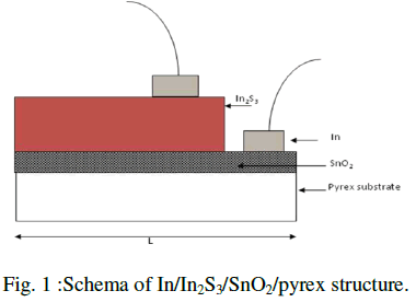 |
| We put them on the sample and we heat the later to about 180°C to ensure diffusion. An impedance analyser was used to collect impedance measurements over a wide frequency range. We employ a parallel mode to measure both conductance G and capacitance C using an alternating signal with amplitude of 50 mV. |
2. Film characterization: |
| The deposited films were characterized using X-ray diffractometer (XRD), scanning electron microscopy (SEM), optical transmission spectra, hall effect and impedance spectroscopy. |
| XRD measurements were performed onD8 Advance diffractometer with CuKïÃÂá monochromatic radiation (ïÃÂì = 1.5418 Å). Surface morphology was examined using a hight resolution SEM type Nanoscope III (Veeco 3100).Optical transmittance and reflectance spectra of the films were measured in the wavelength range of 300–1800 nm on a UVVIS- NIR spectrophotometer (type Shimadzu) equipped with an integrating sphere. Electrical measurements were studied with impedance spectroscopy (HPLF 4192A) analyser in order to collect impedance measurements over a wide frequency range. Conductivity of In2S3 films has been determined using the hot probe method and found to be n-type. |
RESULTS AND DISCUSSION |
X-ray diffraction analysis: |
| The phase structure of the product was characterized by XRD analysis. Fig. 2 shows the typical XRD patterns of the sample prepared at 240°C. Seven pronounced diffraction peaks appear in the 10–70° 2ïÃÂñ range. All the peaks of the XRD pattern were indexed for each reflection of the compound and seen on the pattern. This one shows several peaks that corresponding to be related to cubic In2S3. |
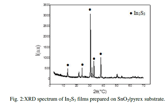 |
| All the reflection peaks can be readily indexed as cubic phase of ïÃÂâ-In2S3 structure (JCPDS). No characteristic peaks arising from the possible impurities are visible, such as InS, In2O3 and other phases of In2S3. And the peaks are considerably strong and narrow, which indicate that the product is well crystallized. |
| The average grain size was calculated using Scherrer’s formula [23]: |
 |
| Where λ is the X-ray wavelength (1.5418Å), βis the maximum of the Bragg diffraction peak and β is the line width at half maximum (in radians). |
2 Morphological analysis: |
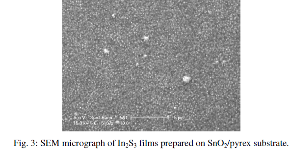
| Scanning electron micrographs are helpful to elucidate the topographic properties of the grown films surface. Fig. 3 shows the scanning electron micrograph of In2S3/SnO2/pyrex describing their surface topography. It is clearly seen from the photograph that the surface is homogeneous with high density and covered substrate well. |
| It can be seen that the surface is very compact which can be explained by the effect of the substrate nature. In fact, the SnO2 substrate was used to achieve the ohmic contact in the CuInS2/In2S3 solar cells where CuInS2 is the absorber material and In2S3 the optical window. |
 |
3 Optical analysis: |
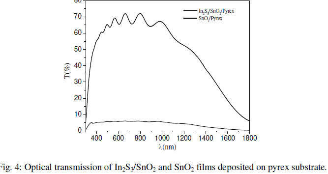
| Optical transmission spectra of In2S3/SnO2and SnO2films in the range of 300–1800 nm for as-deposited indium sulfide films are shown in Fig.4. The sample is found to show a sharp UV cut-off at about 370 nm. The transmittance of samples in the visible spectral range (400–800 nm) is above 70% for SnO2 films with large amplitude interference fringe indicating a highly homogeneity of films. The transmittance in the near-infrared region decreases owing to interaction with free-carriers in the SnO2 suggesting the presence of high shallow state density. For In2S3/SnO2/pyrex the transparency of the film is reduced due to their thicker nature and the transmission is lower than 10% depending on the thickness of the films. |
 |
4 Impedance spectrum analysis: |
| The electrical behaviour of the system has been studied over a wide range of frequency (60–108Hz) at ambient temperature in dark and illumination using impedance spectroscopy technique. This technique enables us to separate the real and imaginary components of the electrical parameters and hence provides a true picture of the materials properties. |
| Fig.5 shows the frequency dependence of the conductance at dark and illimunation. |
| The conductance was calculated using the following formula [24]: |
 |
| Where G(ω)is the conductance of In2S3sample. It demonstrates a monotonous increase with frequency over the high frequency range (>10Hz) side. The conductance patterns show a frequency independent plateau in the low frequency region and exhibits dispersion at higher frequencies. This behavior obeys the universal power law [25, 26], |
| Where Gdc is the dc conductance (frequency independent plateau in the low frequency region), A is the pre-exponential factor and m is the fractional exponent between 0 and 1, corresponding to a hopping process. |
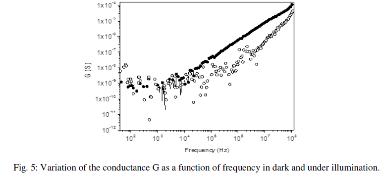 |
| Conductance spectra can be splitted into two parts. First, at low frequency a plateau appears for both cases. A rise in the conductance value with temperature indicates that electrical conductance in the material is a thermally activated process. The conduction is due only to the relaxation process and polarization field. |
| Therefore the charge carrier transport could take place via the hopping between the localized states. Some of the trap states created by disordered atoms and incomplete bonding between them could be filled by the carriers depending on their distribution in the band gap and subsequently got charged. The empty states may capture electrons from the charged states and hence the conduction would be followed by the hopping of charge carriers from filled trap states to empty trap states. |
| Second, at high frequency part, the conductance G proves the existence of a hopping mechanism. The frequency at which a change in the slope of the conductance spectrum occurs is conventionally known as the “hopping frequency”. On the other hand, conductance spectra approach close to each other at high frequency. This may be due to the electrical charge localization [27]. |
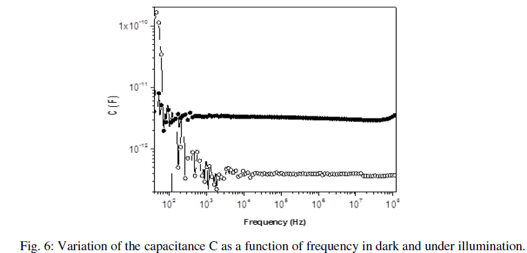
| Fig. 6 shows the capacitance spectra versus frequency. Similar results were practically obtained at room temperature in dark and illumination conditions. The capacitance slowly decays over a broad frequency range 100 Hz- 100 kHz. The increase of the capacitance is associated with polarization due to the transfer of photo-generated electrons and holes. |
 |
5 Hall Effect: |
| The resistivity, the mobility and the concentration of carriers are represented in the table 1. We note that hall mobility is high for films deposited on SnO2/Pyrex. Indeed the influence of the support is clear for the layers of indium sulphide. So, for the amorphous supports (glass), it is formed a fine layer of the compound due to the strong density of constraints on the support. In the partially directed supports, the hall mobility of carriers is relatively better than that of the layers deposited on amorphous support. The concentration carrier is also significant for the two series of samples. The latter which is an effective measurement of the hall constant, approaches the concentration carriers of the monocrystal. The hall mobility and resistivity are ameliorating for layers deposited on SnO2/pyex. |
| The hall effect study confirmed that layers have a very significant density out of carrier’s loads indicating a semiconductrice nature of type n. |
 |
CONCLUSION |
| In2S3 layers were prepared by vacuum thermal evaporation methodon SnO2/pyrex at 240°C. These layers are adherent and homogeneous in appearance. XRD studies revealed that In2S3 film is crystallized without any secondary phases. SEM measurements indicated that the films are homogenous and formed with a crystallites separated by grain boundaries. Impedance analysis revealed that conduction is due to the relaxation process and polarization field and the capacitance to the transfer of photo-generated electrons and holes. Hall effect prove that mobility depend strongly to substrate and confirm n-type nature of film. |
| In2S3 layers with these properties suitables for their application as buffer layers in photovoltaic devices. Future works will be focussed on the optimization of the optical parameters without deteriorate the electronic and structural ones. |
References |
|