ISSN ONLINE(2319-8753)PRINT(2347-6710)
ISSN ONLINE(2319-8753)PRINT(2347-6710)
Rani.S 1, Shanthi.J 2
|
| Related article at Pubmed, Scholar Google |
Visit for more related articles at International Journal of Innovative Research in Science, Engineering and Technology
Cadmium selenide (CdSe) thin films on glass substrates were prepared by physical vapor deposition under vacuum by electron beam evaporation technique at room temperature (RT) and annealed at 100, 200 and 300 o C respectively. Photoluminescence (PL) spectra were recorded in the wavelength region of 470 to 600 nm. The result shows that the EB evaporated CdSe films have strong PL in the green region and the emission band values observed in PL studies are very much blue shifted. Raman result shows that the peak corresponding to the second order (2 LO) and third order (3 LO) phonon modes at 416 and 625 cm-1 respectively. The first order LO phonon mode is not observed. The surface morphological quality of electron beam evaporated CdSe films were analyzed by atomic force microscopy (AFM).
Keywords |
| CdSe films; Electron beam evaporation; annealed;Raman;PL spectra;AFM |
I. INTRODUCTION |
| During the past few decades, there has been increasing interest in the deposition and characterization of II–VI group chalcogenide semiconductor compound thin films because of their wide application in various fields of optoelectronic technology. Among II-VI group, CdSe is considered to be a potential candidate for various applications such as photo electrochemical solar cells [1], thin film transistors, sensors, lasers, photoconductors, and gamma ray detectors [2–4] because of having high efficiency of radiative recombination, high absorption coefficient, high photosensitivity, direct band gap corresponding to a wide spectrum of wavelengths from ultraviolet to infrared regions [5-7] and quantum size effect [8]. |
| The deposition parameters such as temperature, thickness and deposition time influence the formation of nanocrystalline thin films and crystallite size, which in turn engineer the band gap of the material [9]. In present investigation we have used electron beam evaporation technique and optimized for deposition of CdSe thin films. Due to high power density and wide range of controlled evaporation, the electron beam evaporation technique is more suitable for the deposition of CdSe thin films. During deposition of film, evaporate material is placed in water cooled graphite crucible, so that only its upper surface gets high temperature. Thus, metallurgical reaction between evaporate material and crucible is eliminated. This technique provides economical and efficient use of evaporate material enabling constant rate of deposition. |
| CdSe films have been prepared by EB evaporation technique on glass substrates at room temperature and annealed at different temperatures in the range RT – 300 °C, were characterized by Raman, photoluminescence and surface morphological analysis. The results are presented and discussed in detail. |
II.MATERIALS AND METHODS |
| CdSe films were deposited using Hind Hivac electron beam evaporation unit on glass substrates at different substrate temperatures in the range RT – 300 °C. Substrate temperature was fixed on the basis of the TGA data of the CdSe powder. The films were deposited with 5 kV and 10 mA under a vacuum of 10-6 Torr. Film thickness was measured by the stylus Profilometer (Mitutoyo). |
| Raman studies were made using Renishaw Invia Laser Raman microscope using 18 mW 633 nm He-Ne laser. PL studies were made using Varian Cary Eclipse Fluorescence Spectrophotometer. Surface morphology of the films was studied by Nanoscope E-3138j AFM/STM Molecular Imaging system atomic force microscope. |
III. RESULTS AND DISCUSSION |
1. PHOTOLUMINESCENCE (PL) STUDIES OF CdSe FILMS |
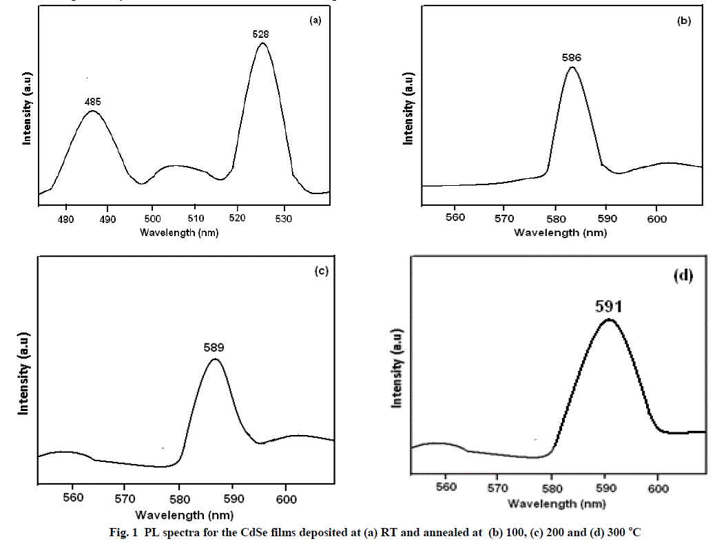
| PL spectra of CdSe films deposited at different temperatures of RT and annealed at 100, 200 and 300 oC were recorded by PL spectrophotometer. The emission spectra were recorded in the range from 470 to 600 nm. CdSe is a direct band gap semiconductor film. Due to its hexagonal crystal field and spin-orbit interaction, the valence band is split into three doubly degenerate states [10]. |
| The PL spectra of CdSe thin films deposited at RT and annealed at 100, 200 and 300 °C are shown in figure 1 a, b, c and d respectively which were recorded at room temperature. |
 |
| CdSe films deposited at RT have lower grain size whose PL spectrum (Fig. 1 a) shows an intense band in the green region (528 nm) and a less intense in the blue region (485 nm). The CdSe films deposited at 100, 200 and 300 °C have intense green bands at 586, 589 and 591 nm respectively. These results shows that the EB evaporated CdSe films have strong PL in the green region and the emission band values observed in PL studies are very much blue shifted. Such a large stokes shift between the optical absorption spectrum and PL emission band may be attributed to the presence of one deep trapping site and electron hole recombination via trap state or imperfection site (donor here) [11]. Such lattice phenomena are observed in nanomaterials and these results confirm the nano crystalline nature of the EB evaporated CdSe films in the present study. Deep states in nanocrystalline materials are mainly associated with stoichiometric defects, dangling bonds or external ad atoms such as oxygen [44] |
2. RAMAN SPECTROSCOPY STUDIES OF CdSe FILMS |
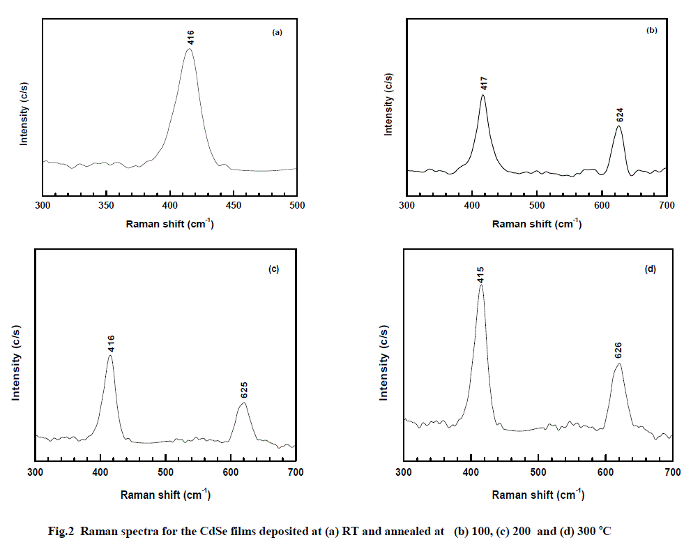
| Figure 2 shows the Raman spectra for the CdSe films deposited on glass substrates at RT, and annealed at 100, 200 and 300 oC. The standard Raman spectrum for bulk CdSe is characterized by two futuristic peaks, one at 209 cm-1 and its overtone at 420 cm-1 which are assigned to the longitudinal optical (LO) phonon mode [13-15]. |
 |
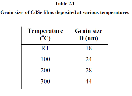
| The Raman spectrum for bulk CdSe is characterized by two peaks, one at 209 cm-1 and its overtone at 410 cm-1 which are assigned to the longitudinal optical (LO) phonon mode [16, 17]. The CdSe thin films, deposited in the present study, show the peak corresponding to the second order (2 LO) and third order LO (3 LO) phonon modes at 416 and 625 cm-1 respectively. The first order LO phonon mode at 209 cm-1 is not observed. It is reported that the first order LO is observed for CdSe nanoparticles with crystallite sizes below 18.3 nm prepared by chemical route [18]. Further, it is also mentioned that chemically prepared CdSe samples with bigger nanocrystals show second - order 2 LO phonon band near 420 cm-1 followed by a weak peak near 620 cm-1 attributed to 3 LO phonon scattering. These results show that our CdSe films should have nanocrystallites in the range greater than 18.0 nm. This is supported by the observed grain size in the range of about 18 – 44 nm as shown in the table. |
 |
| Further, the full width at half maximum (FWHM) of the CdSe LO phonon peaks are nearly the same for all the films deposited at RT and 300 °C. Except for the reduction in intensity of the peaks with increased substrate temperature, no change in FWHM and no shift in peak values confirm the uniform size distribution of the grains for the EB evaporated CdSe films in our study. Desmica-Frankovic et al [19] have studied CdSe Quantum dots (QDs) prepared by ion beam synthesis in which films showed a LO peak at 255 cm-1 corresponding to Cd – deficiency and formation of selenium clustering in thin CdSe films. This also confirms that we are able to prepare stoichiometric CdSe films without any selenium clustering. |
3. SURFACE MORPHOLOGY ANALYSIS OF CdSe FILMS |
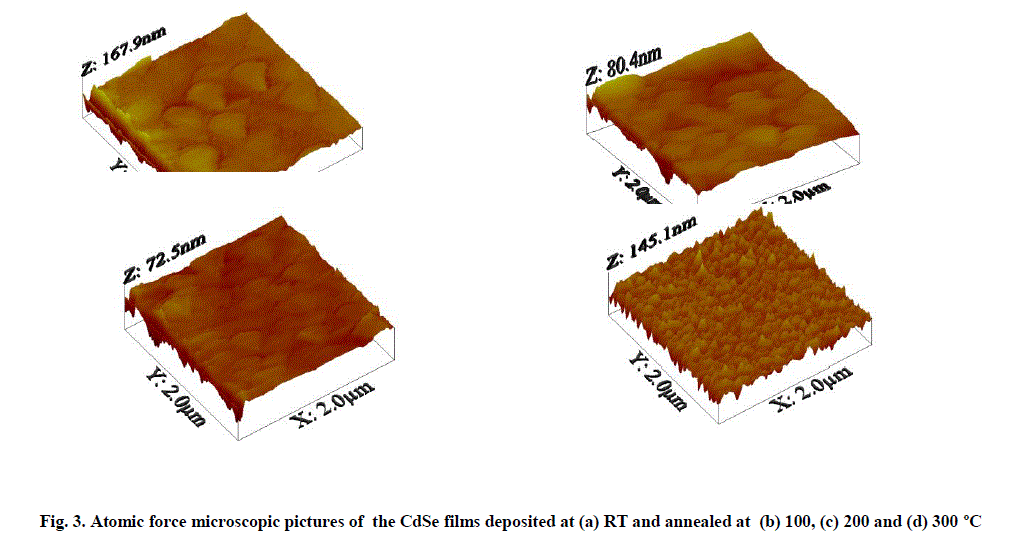
| Study of surface smoothness and grain size variation with temperature is an important observation for developing device quality films. AFM surface morphological property have been studied and presented here. Figure 3. a, b, c and d represent the three dimensional (3D) AFM images of CdSe films deposited at RT, and annealed at 100, 200 and 300 oC respectively. Three dimensional (3D) topography of these CdSe films which shows very clearly the ups and downs and the presence of pin holes or other defects. |
 |
| Presence of agglomerated crystallites are confirmed for the films deposited at RT and 300 oC and the films deposited at 100 and 200 oC have uniform dispersion of small size grains throughout the surface with size distribution of 40 – 220 nm. The film matrix was found to have some spherical particles embedded into the background fine grained matrix. These granual particles may be CdSe agglomerates deposited over the uniformly spread CdSe nano particles. These are observed in large number in the films deposited at RT. An increase of grain size from 40 to 220 nm is observed as the substrate temperature increase from RT to 300 oC. |
| For a detailed study on specific roughness or average roughness properties of CdSe surface and their variation with deposition temperatures were calculated from AFM pictures. This will provide valuable information on the height deviation of the roughness profile and on its lateral distribution [20, 21]. From the line profile analysis, the average roughness values calculated are 0.34, 0.21, 0.25 and 0.35 nm for the CdSe films deposited at RT, 100, 200 and 300 oC respectively. The vertical surface roughness deviation are higher for the CdSe films deposited at RT and 300 oC than those deposited at 100-200 oC. The CdSe films deposited at 100 oC shows the most uniform surface with minimum surface average roughness value. These observations show that CdSe films deposited at 100 oC have the device quality surface which will be suitable for developing photo electrochemical (PEC) solar cells. |
V. CONCLUSION |
| EB evaporated CdSe films have strong PL in the green region and indicated two peaks. Raman spectra measurements showed the presence of 2LO and 3LO phonon peaks. Surface morphology results show that the CdSe films deposited at 100 oC shows the most uniform surface with minimum surface average roughness value of 0.21 nm. These observations show that CdSe films deposited at 100 oC have the device quality surface which will be suitable for developing photo electrochemical (PEC) solar cells. |
References |
|